
 My Inquiry
 My Account


NXP Semiconductors PTN3460BS/F3Y
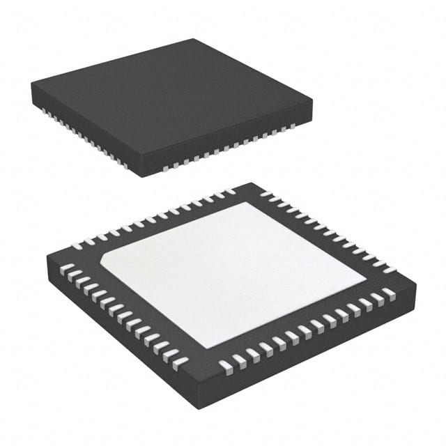
- Part No.:
- PTN3460BS/F3Y
- Manufacturer:
- NXP Semiconductors
- Category:
- Specialized
- Package:
- 56-VFQFN Exposed Pad
- Datasheet:
-
 PTN3460BS/F3Y.pdf
- Description:
- IC INTFACE SPECIALIZED 56HVQFN
- Quantity:
- Payment:

- Shipping:

Inventory:1,550
Please send an inquiry. Send us your inquiry, and we will respond immediately.
Product details
Overview
PTN3460BS/F3Y from NXP Semiconductors is an embedded DisplayPort (eDP) to LVDS bridge IC that converts DP v1.2/eDP v1.2 video streams into dual-bus or single-bus LVDS output for driving high-resolution display panels. It supports 1- or 2-lane DP input at 1.62 Gbit/s or 2.7 Gbit/s, LVDS pixel clock up to 112 MHz, 18/24 bpp color depth, and VESA/JEIDA data packing - enabling 1920×1200@60 Hz in dual-bus mode for notebook and AIO platforms.
For engineers reviewing the PTN3460BS/F3Y datasheet, PTN3460BS/F3Y pinout, PTN3460BS/F3Y application, or PTN3460BS/F3Y equivalent, key selection considerations include eDP-to-LVDS protocol conversion fidelity, EDID ROM emulation capability, programmable LVDS signal swing and clock spreading, panel power sequencing control via PVCCEN/BKLTEN/PWMO, and multi-mode configuration via CFG pins or I2C/AUX interfaces.
Technical Context
The PTN3460BS/F3Y implements a full DisplayPort receiver with Auto Receive Equalization, Clock Data Recovery (CDR), and support for Fast/Full Link training per VESA DP v1.2 and eDP v1.2 standards. Its integrated DPCD registers (v1.2) enable native AUX and I2C-over-AUX transactions for link setup, EDID-DDC access, and firmware-controlled panel initialization.
On the LVDS side, it delivers two independent LVDS buses (odd/even), each supporting up to four differential data pairs plus clock, with programmable channel swapping, polarity inversion, and center-spread clock modulation (32.9 kHz). The embedded microcontroller and on-chip NVM allow runtime reconfiguration and firmware updates without external memory.
Key Specifications
| Parameter | Value and Actual Design Meaning |
|---|---|
| Display Interface | eDP v1.2 / DP v1.2 compliant receiver with 1–2 lane Main Link and 1 Mbit/s AUX channel |
| LVDS Output Capability | Dual-bus LVDS supporting 1920×1200@60 Hz at 112 MHz pixel clock, 18/24 bpp, VESA or JEIDA format |
| Power Supply Options | Single 3.3 V supply (internal 1.8 V regulator enabled) or dual 3.3 V/1.8 V supplies (EPS_N pin controlled) |
| EDID Handling | On-chip EDID ROM emulation supporting up to seven EDID structures (v1.3), eliminating need for external EEPROM |
| Configuration Interfaces | Multi-level CFG pins (CFG1–CFG4), I2C-bus slave (100/400 kbit/s), and DP AUX channel for register access and DDC |
| Operating Temperature | 0 °C to +70 °C - validated for commercial notebook and AIO platform environments |
| ESD Robustness | 8 kV HBM, 1 kV CDM - suitable for assembly and field-reliable display subsystems |
Pinout & Package
HVQFN56 package (7 mm × 7 mm, 0.4 mm pitch) with exposed center pad for thermal relief and electrical grounding. Pin count: 56 terminals; max height: 1 mm.
| Pin/Terminal | Circuit Role | Design Meaning |
|---|---|---|
| DP0_P / DP0_N DP1_P / DP1_N | DP Main Link differential inputs | AC-coupled 2-lane DP receiver interface; supports 1.62/2.7 Gbit/s; internal 50 Ω termination |
| AUX_P / AUX_N | DP AUX channel differential I/O | Supports Native AUX and I2C-over-AUX for DPCD access and EDID-DDC communication |
| LVSAE_P/N – LVSDE_P/N LVSAO_P/N – LVSDO_P/N | Dual-bus LVDS data outputs (even/odd) | Eight total LVDS data pairs; configurable for JEIDA/VESA packing, channel swapping, and polarity inversion |
| LVSCKE_P/N / LVSCKO_P/N | LVDS clock outputs (even/odd) | Programmable center-spread clock (0–1 % depth) to reduce EMI; supports up to 112 MHz |
| PVCCEN / BKLTEN / PWMO | Panel control outputs | CMOS signals for sequenced panel power enable, backlight enable, and PWM dimming control |
| RST_N / PD_N / DEV_CFG | System control inputs | Active-low reset, deep power-down, and I2C address/configuration mode selection |
Key Features
| Feature | Design Value |
|---|---|
| Embedded microcontroller + on-chip NVM | Enables field-upgradable firmware and persistent configuration storage without external memory |
| EDID ROM emulation | Supports up to seven distinct EDID structures (v1.3), allowing plug-and-play compatibility with panels lacking EDID EEPROM |
| Programmable LVDS signal swing | Three selectable levels (250/300/400 mV) to compensate for PCB trace loss or optimize power consumption |
| Firmware-controlled panel sequencing | Configurable timing for PVCCEN, BKLTEN, and PWMO enables robust power-up/down sequences aligned with eDP v1.2 requirements |
| Flexible configuration options | Simultaneous support for multi-level CFG pins, I2C-bus (0x40h/0xC0h), and DP AUX for system integration across BIOS, GPU driver, and hardware layers |
Applications
| High-Resolution Notebook Displays | All-in-One (AIO) Desktop Panels |
|---|---|
Use Scenario: Converting eDP output from Intel Core i-series CPU/GPU to drive 1920×1200 LVDS panels in thin-and-light notebooks. IC Role / Device Role / Timing Role: Protocol bridge translating eDP v1.2 packetized video into synchronized LVDS pixel/data/clock signals with precise DE/HSYNC/VSYNC timing. Use Value: Enables native resolution support without custom FPGA logic; EDID emulation avoids BIOS modifications for non-standard panels. |
Use Scenario: Interfacing AMD Ryzen APUs to dual-channel LVDS displays in compact AIO systems requiring low EMI and flexible layout routing. IC Role / Device Role / Timing Role: Dual-bus LVDS transmitter with programmable channel swapping and clock spreading to meet stringent EMC requirements. Use Value: Reduces board-level filtering components via center-spread clock (32.9 kHz); LVDS bus flexibility simplifies PCB routing around mechanical constraints. |
| Netbook and Embedded Panel Systems | eDP-to-LVDS Migration Platforms |
Use Scenario: Replacing legacy LVDS transmitters in cost-sensitive netbooks using eDP-capable SoCs. IC Role / Device Role / Timing Role: Drop-in eDP receiver with backward-compatible LVDS output, supporting both 18 bpp (low-cost panels) and 24 bpp (wide-gamut displays). Use Value: Eliminates need for external level shifters or timing controllers; single-supply operation (3.3 V only) reduces BOM count. |
Use Scenario: Upgrading existing LVDS-based designs to leverage newer eDP-enabled processors while retaining legacy display modules. IC Role / Device Role / Timing Role: Protocol translator with configurable data packing (VESA/JEIDA) and pixel clock range (25–112 MHz) to match diverse panel TCONs. Use Value: Avoids panel redesign; firmware-configurable parameters allow one hardware design to support multiple display vendors. |
Equivalent & Alternatives
The following parts are listed as comparable options for similar eDP-to-LVDS bridge applications.
| Alternative Part | Technical Difference | Application Difference | Selection Advice |
|---|---|---|---|
| TI SN75DP130 | Single-lane DP input only; no built-in EDID emulation; requires external EEPROM for EDID | Targeted at lower-resolution panels (< 1366×768); lacks dual-bus LVDS and panel power sequencing outputs | Select when cost sensitivity outweighs resolution and panel compatibility requirements |
| Parade Technologies PS8315 | Supports DP 1.2a but no eDP authentication (ASSR/Enhanced Framing); no on-chip NVM or firmware update capability | Used in industrial HMIs with fixed panel configurations; limited configurability via I2C only (no AUX-based DPCD access) | Select when eDP security features and field firmware updates are not required |
Compared with SN75DP130 and PS8315, PTN3460BS/F3Y uniquely integrates EDID ROM emulation, eDP v1.2 authentication, dual-bus LVDS with 112 MHz clock, and firmware-upgradable NVM - making it the only option supporting full 1920×1200@60 Hz in commercial notebooks with zero-EEPROM panel bring-up.
Availability
PTN3460BS/F3Y is available at Aetrix Electronics and suitable for notebook platforms, AIO desktop systems, and netbook designs requiring stable component supply, long-term display interface continuity, and eDP-to-LVDS protocol translation with embedded panel control.
Supply support for PTN3460BS/F3Y includes scheduled delivery planning, volume procurement assistance, BOM continuity management, traceable sourcing, and lifecycle availability coordination for OEM customers, industrial embedded developers, connected-device designers, and electronics production programs.
Manufacturer
NXP Semiconductors is a global semiconductor company specializing in secure connectivity solutions for automotive, industrial, and consumer electronics, with leadership in interface, analog, and embedded processing technologies.
The PTN3460BS/F3Y belongs to NXP's display interface product line, designed specifically to simplify eDP-to-LVDS migration in space-constrained, power-sensitive computing platforms where panel compatibility, firmware flexibility, and EMI compliance are critical.
FAQ
What display resolutions does the PTN3460BS/F3Y support?
The PTN3460BS/F3Y supports up to 1920×1200@60 Hz in dual LVDS bus mode at 112 MHz pixel clock, with 18 bpp or 24 bpp color depth. It also supports lower resolutions including 1366×768 and 1024×768 in single-bus mode. Resolution capability depends on configured LVDS bus count, pixel clock frequency, and data packing format (VESA or JEIDA), all programmable via CFG pins or AUX/I2C interfaces.
Does PTN3460BS/F3Y require an external EDID EEPROM?
No, PTN3460BS/F3Y does not require an external EDID EEPROM. It includes on-chip EDID ROM emulation supporting up to seven distinct EDID structures (v1.3), enabling plug-and-play operation with panels lacking EDID memory. This eliminates BIOS modifications and external component costs while maintaining full DDC/EDID compliance for eDP source negotiation.
How is the PTN3460BS/F3Y powered - single or dual supply?
The PTN3460BS/F3Y supports both configurations: a single 3.3 V supply (with internal 1.8 V regulator enabled via EPS_N pin left open or pulled HIGH), or dual 3.3 V/1.8 V supplies (with EPS_N pulled LOW). Power supply selection is hardware-configured and affects internal regulator operation - verified in the datasheet Section 2.5 and Table 2 pin description for EPS_N (Pin 56).
Can PTN3460BS/F3Y be configured without firmware updates?
Yes, PTN3460BS/F3Y supports hardware-based configuration via multi-level CFG pins (CFG1–CFG4) for LVDS bus count, data format (VESA/JEIDA), clock spread depth, and output swing - enabling full operation without firmware intervention. Firmware updates are optional and used only for advanced features like custom EDID structures or enhanced power sequencing, stored in on-chip NVM.
What is the role of the HPDRX pin on PTN3460BS/F3Y?
The HPDRX pin on PTN3460BS/F3Y is a Hot Plug Detect output signal sent to the eDP source (e.g., GPU). It remains LOW during power-up and initialization, then transitions HIGH to indicate readiness. Internally pulled down (>100 kΩ), it prevents false HPD events before device initialization completes - ensuring reliable link training and avoiding source-side errors during boot.
PTN3460BS/F3Y Specifications
- Product attributes
- Attribute value
- Manufacturer:
- NXP Semiconductors
- Series:
- -
- Package/Case:
- 56-VFQFN Exposed Pad
- Packaging:
- Tape & Reel (TR)
- Product Status:
- Active
- Applications:
- LVDS
- Interface:
- -
- Voltage - Supply:
- 3.3V
- Supplier Device Package:
- 56-HVQFN (7x7)
- Grade:
- -
- Qualification:
- -
- Mounting Type:
- Surface Mount
PTN3460BS/F3Y FAQ
1.How can I place an order for PTN3460BS/F3Y through Aetrix?
Please submit a Request for Quotation (RFQ) for PTN3460BS/F3Y on Aetrix. Our sales agent will provide a competitive quotation and guide you through the order confirmation once you accept the terms.
2.Are the price and stock information for PTN3460BS/F3Y reliable?
The price and inventory of PTN3460BS/F3Y are updated periodically and may fluctuate due to market conditions. Stock and pricing data are typically refreshed every 24 hours. Quotation validity for PTN3460BS/F3Y is usually 5 days.
3.What payment methods are accepted for PTN3460BS/F3Y?
We accept Wire Transfer, PayPal, Credit Card, Western Union, MoneyGram, and Escrow for PTN3460BS/F3Y transactions.
Note: Certain payment methods may incur a processing fee.
4.How is shipping managed for PTN3460BS/F3Y?
PTN3460BS/F3Y orders can be shipped via leading logistics carriers, including DHL, UPS, FedEx, TNT, or Registered Mail.
Once your PTN3460BS/F3Y order is processed, you will receive an email with the shipment details and tracking number.
Note: Tracking information may take up to 24 hours to appear. Express delivery typically takes 3–5 business days.
5.How can I obtain technical support or documentation for PTN3460BS/F3Y?
For technical support, including PTN3460BS/F3Y datasheets, pinout diagrams, or application guidance, please contact our engineering support team. They can provide detailed documentation and assistance for your PTN3460BS/F3Y requirements.
6.How does Aetrix verify that PTN3460BS/F3Y is sourced from the original manufacturer or authorized distributors?
All PTN3460BS/F3Y products on Aetrix are procured from qualified distributors and authorized channels. Our dedicated quality assurance team conducts strict verification, including traceability checks and, if necessary, third-party testing. This ensures that PTN3460BS/F3Y meets industry standards.
7.What is the process for return or replacement of PTN3460BS/F3Y?
All PTN3460BS/F3Y units undergo pre-shipment inspection (PSI). If there is an issue with PTN3460BS/F3Y, returns or replacements are accepted under the following conditions:
1.Quantity discrepancies, incorrect items, or visible external defects (such as breakage or corrosion), acknowledged by Aetrix.
2.The issue is reported within 90 days of delivery.
3.The PTN3460BS/F3Y part is unused and in its original packaging.
Return procedure for PTN3460BS/F3Y:
1.Submit a request within 90 days.
2.Obtain a Return Material Authorization (RMA) from Aetrix.
PTN3460BS/F3Y Tags

-
NVT4857UKAZ
NXP Semiconductors

-
TCA8418RTWR
Texas Instruments

-
PCA9546APWR
Texas Instruments

-
MD0100N8-G
Microchip Technology

-
PCA9548APW,118
NXP Semiconductors

-
PCA9540BDP,118
NXP Semiconductors

-
PCA9548APWR
Texas Instruments

-
PCA9546APW,118
NXP Semiconductors

-
PTN3360DBS,518
NXP Semiconductors

-
PCA9546ABS,118
NXP Semiconductors

-
PCA9518PWR
Texas Instruments

-
PCA9545APW,118
NXP Semiconductors
Tech Hub

A practical engineering guide to 3.3V and 5V logic compatibility, input thresholds, resistor dividers, translator ICs, MOSFET level shifting, I2C pull-ups, timing limits and power-sequencing risks.

The 74HC595 uses push-pull logic outputs, while the TPIC6B595 uses 50 V open-drain DMOS sinks for higher-power loads. This guide compares timing, current limits, 3.3 V interfacing, load wiring, thermal…

The 74HC595 converts serial data into eight stable parallel outputs. This guide covers pin functions, shift and storage timing, OE and MR behavior, drive-current limits, cascading, voltage compatibilit…

A technical comparison of level-sensitive latches and edge-triggered flip-flops, covering timing windows, setup and hold limits, master–slave operation, time borrowing, race-through, HDL inference and…

A D latch stores one bit while Enable controls when data can pass. This reference covers gate-level operation, truth tables, transparency, setup and hold timing, LE versus OE, common ICs and practical …

An SR latch stores one bit through cross-coupled feedback. This engineering reference covers NOR and NAND implementations, truth tables, forbidden-state recovery, gated operation, switch debouncing, fa…

Latch circuits retain one bit through feedback. This technical reference covers SR and D latches, truth tables, transparency, timing limits, latch-versus-flip-flop behavior, applications and common log…

An engineering guide to LED driver operation, constant-current and constant-voltage outputs, linear and switching topologies, dimming, IC selection, calculations, replacement compatibility, and fault c…

Operational amplifier guide covering op amp basics, feedback, ideal vs real op amps, common configurations, buffer circuits, offset, bias current, gain-bandwidth, slew rate, rail-to-rail limits and sel…

Jumper cables guide covering safe connection order, red and black clamp placement, final ground connection, cable gauge, length, clamp quality, copper vs CCA cables, jump starter comparison and battery…


