
 My Inquiry
 My Account


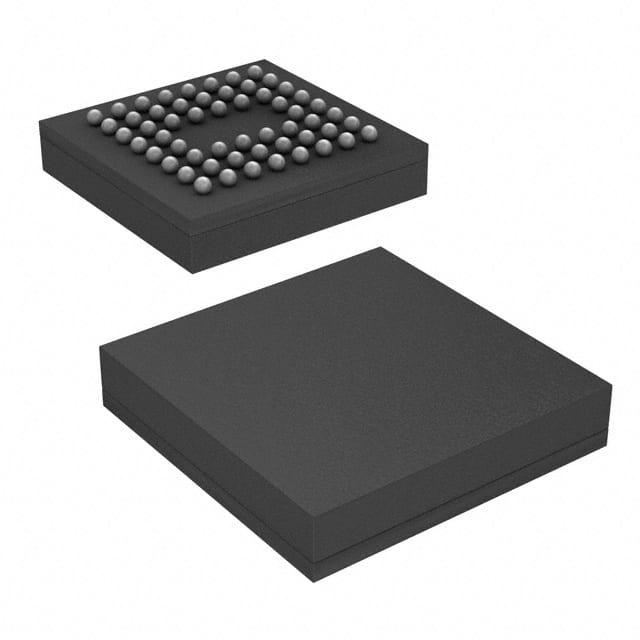
NXP Semiconductors PTN3700EV/G,118
- Part No.:
- PTN3700EV/G,118
- Manufacturer:
- NXP Semiconductors
- Category:
- Video Processing
- Package:
- 56-VFBGA
- Datasheet:
-
 PTN3700EV/G,118.pdf
- Description:
- IC VIDEO INTERFACE 56VFBGA
- Quantity:
- Payment:

- Shipping:

Inventory:3,461
Please send an inquiry. Send us your inquiry, and we will respond immediately.
Product details
Overview
PTN3700EV/G,118 from NXP Semiconductors is a 1.8 V configurable mobile interface link bridge IC that operates as either a transmitter-serializer or receiver-deserializer for RGB888 video data. It supports 1–3 subLVDS serial lanes, delivers up to 1.95 Gbit/s aggregate bandwidth, and implements parity encoding/decoding with last-valid-pixel repetition-enabling robust video transmission in high-resolution mobile displays.
For engineers reviewing the PTN3700EV/G,118 datasheet, PTN3700EV/G,118 pinout, PTN3700EV/G,118 application, or PTN3700EV/G,118 equivalent, key selection considerations include lane count configuration (LS[1:0]), FSS/PSS transmission mode selection, TX/RX direction control, and Frame Mixing enablement (FM) in receiver mode for 24-bit-to-18-bit color depth conversion.
Technical Context
The PTN3700EV/G,118 integrates a low-jitter PLL that locks to PCLK in transmitter mode or CLK in receiver mode, generating phase-aligned internal clocks for serialization/deserialization. Its dual transmission protocols-pseudo source synchronous (FSS = LOW) and true source synchronous (FSS = HIGH)-differ fundamentally: the former uses pixel clock edges for frame delineation and requires receiver-side PLL regeneration, while the latter embeds synchronization words and uses DDR bit clock alignment to eliminate false pixel sync and reduce power.
Signal routing flexibility is achieved via TX/RX mode detection and two Pin Select bits (PSEL[1:0]), enabling four distinct pinout configurations per mode to avoid PCB trace crossing. In receiver mode, the patented Advanced Frame Mixing function processes 24-bit input to generate 18-bit output with perceptually preserved 24-bit color depth-specifically for legacy 18-bit display panels.
Key Specifications
| Parameter | Value and Actual Design Meaning |
|---|---|
| Supply Voltage | 1.8 V ±150 mV single supply-enables direct integration into modern low-voltage mobile SoC power domains without level-shifting. |
| Serial Interface | Configurable 1/2/3 subLVDS differential lanes-supports scalable bandwidth from 650 Mbit/s (QVGA) to 1.95 Gbit/s (XGA) without changing physical layer. |
| Parallel Interface | 24-bit RGB888 + HS/VS/DE + A[1:0] CMOS-maintains full compatibility with standard mobile display controllers and timing generators. |
| Power Modes | Shutdown (<3 µA), Standby (<3 µA), Active (15–40 mW)-enables aggressive power gating in battery-constrained portable devices. |
| Frame Mixing | Patent-pending algorithm in receiver mode only-converts 24-bit input to 18-bit output with enhanced color fidelity for cost-optimized 18-bit displays. |
| Parity Handling | Odd parity encoding (TX) and detection (RX) with CPO error flag and automatic last-valid-pixel hold-ensures pixel-level data integrity without system-level retransmission overhead. |
| Operating Temp | −40 °C to +85 °C-qualified for industrial-grade mobile and automotive infotainment display applications. |
Pinout & Package
The PTN3700EV/G,118 is housed in a 56-ball Very Thin Fine-Pitch Ball Grid Array (VFBGA56) package measuring 4 × 4.5 × 0.65 mm with 0.5 mm ball pitch. Pin functions are dynamically mirrored based on TX/RX mode and PSEL[1:0] inputs-enabling flexible PCB layout without signal crossovers.
| Pin/Terminal | Circuit Role | Design Meaning |
|---|---|---|
| TX/RX | Mode Configuration Input | High = Transmitter; Low = Receiver-automatically reconfigures parallel I/O direction and serial I/O polarity to match link topology. |
| LS[1:0] | Lane Count Select | 00=1 lane, 01=2 lanes, 10=3 lanes-sets serialization ratio (30×/15×/10×) and must be matched identically between transmitter and receiver. |
| FSS | Transmission Protocol Select | Low = Pseudo Source Sync (PCLK-referenced); High = True Source Sync (DDR bit clock + embedded sync words)-determines receiver PLL usage and sync reliability. |
| FM | Frame Mixing Enable | Active HIGH only in Receiver mode-activates patented 24-bit→18-bit color processing; inactive in Transmitter mode (tied to GND). |
| CPO | Parity Error Output | Active HIGH indicates odd-parity failure on R/G/B/HS/VS/DE bits-triggers automatic hold of last error-free pixel data at outputs. |
| XSD | Shutdown Control | Active LOW disables all circuitry-reduces current to <3 µA; essential for zero-power standby in always-on display subsystems. |
Key Features
| Feature | Design Value |
|---|---|
| Configurable Tx/Rx Direction | Single device replaces dedicated serializer and deserializer ICs-reduces BOM count and simplifies inventory management for dual-role display interfaces. |
| Programmable Signal Mirroring | PSEL[1:0] + TX/RX auto-mirroring eliminates need for flex-foil flipping or PCB layer swaps-accelerates integration into existing parallel-display designs. |
| True Source Synchronous Mode | FSS=HIGH enables zero-overhead, false-sync-free operation using embedded sync words-removes dependency on PCLK phase stability and reduces EMI sensitivity. |
| Advanced Frame Mixing | Enables 24-bit color perception on 18-bit displays without external LUT or FPGA logic-lowers display module cost while maintaining visual quality in mid-tier smartphones. |
| Differential SubLVDS I/O | Supports 1–3 high-speed differential lanes with integrated slew rate control (F/XS pin)-balances EMI reduction and signal integrity across varying cable/flex lengths. |
Applications
| Smartphone Display Interface | Tablet Video Link |
|---|---|
Use Scenario: Connecting application processor to high-resolution AMOLED panel in compact smartphone form factor with strict EMI and power constraints. IC Role / Device Role / Timing Role: Bidirectional bridge converting parallel RGB888 from AP to serialized subLVDS for noise-immune panel connection; manages pixel clock recovery and parity-checked data flow. Use Value: Enables 720p/1080p display support using only 1–2 subLVDS lanes-reducing flex cable width and connector pin count versus traditional LVDS solutions. | Use Scenario: Interfacing SoC to dual-display subsystem (main LCD + secondary status OLED) in industrial tablet requiring independent timing and low-latency video routing. IC Role / Device Role / Timing Role: Configured as two independent bridges-one as transmitter driving main display, one as receiver capturing camera preview feed-sharing common power domain and control logic. Use Value: Eliminates need for separate serializer/deserializer pairs-reducing board area by 35% and simplifying thermal management in space-constrained tablet chassis. |
| Automotive Instrument Cluster | Portable Medical Monitor |
Use Scenario: Driving TFT-LCD cluster display from MCU in automotive dashboard where temperature range, functional safety, and EMI immunity are critical. IC Role / Device Role / Timing Role: Receiver-mode bridge accepting serialized video from central graphics unit; performs parity checking and Frame Mixing for legacy 18-bit cluster panels. Use Value: Supports −40 °C to +85 °C operation with built-in error resilience-avoids costly display redesign while meeting ISO 11452-4 EMI compliance requirements. | Use Scenario: Transmitting real-time ultrasound imaging data from FPGA-based acquisition engine to high-brightness clinical display in handheld diagnostic device. IC Role / Device Role / Timing Role: Transmitter-mode bridge serializing 24-bit RGB video at 60 fps with embedded parity-ensuring pixel-perfect image fidelity over noisy medical-grade flex cables. Use Value: Guarantees zero-frame-drop transmission via last-valid-pixel hold on parity errors-critical for diagnostic accuracy where missing pixels could mask pathology indicators. |
Equivalent & Alternatives
The following parts are listed as comparable options for similar mobile video interface bridge applications.
| Alternative Part | Technical Difference | Application Difference | Selection Advice |
|---|---|---|---|
| THCV216 (Texas Instruments) | Fixed transmitter-only function; no receiver mode or Frame Mixing; uses LVDS not subLVDS; higher 3.3 V supply requirement. | Requires separate deserializer for bidirectional links; incompatible with 1.8 V mobile SoCs; limited to simpler display topologies. | Select when only unidirectional high-speed LVDS transmission is needed and 3.3 V rail is available. |
| SN65LVDS31 (TI) | Dedicated 4-channel LVDS serializer; no parallel RGB interface, no parity, no programmable lanes or FSS/PSS modes; 3.3 V only. | Suitable only as raw serializer for custom protocols-not a drop-in replacement for SMILi-compliant RGB888 bridging. | Choose for non-standard video formats where full SMILi compliance and RGB timing semantics are unnecessary. |
Compared with THCV216 and SN65LVDS31, the PTN3700EV/G,118 uniquely combines bidirectional operation, subLVDS low-power signaling, 1.8 V compatibility, and Frame Mixing-making it the sole option for cost-sensitive, power-constrained mobile displays requiring 24-bit color on 18-bit hardware.
Availability
PTN3700EV/G,118 is available at Aetrix Electronics and suitable for high-resolution mobile phones, portable medical monitors, automotive instrument clusters, and industrial tablets requiring stable component supply across extended temperature ranges and long production lifecycles.
Supply support for PTN3700EV/G,118 includes scheduled delivery planning, volume procurement assistance, BOM continuity management, traceable sourcing, and lifecycle availability coordination for OEM customers, industrial embedded developers, connected-device designers, and electronics production programs.
Manufacturer
NXP Semiconductors is a global semiconductor leader specializing in secure connectivity solutions for automotive, industrial, and mobile applications-with deep expertise in interface IP and low-power mixed-signal design.
The PTN3700 product line was developed specifically for energy-efficient, high-fidelity mobile display interconnects compliant with the open Simple Mobile Interface Link (SMILi) specification-targeting smartphone, tablet, and automotive HMI markets.
FAQ
What is the primary function of the PTN3700EV/G,118 in a mobile display system?
The PTN3700EV/G,118 serves as a configurable bridge IC that either serializes parallel RGB888 video data (transmitter mode) or deserializes high-speed subLVDS streams (receiver mode). It supports 1–3 lanes, parity protection, and Frame Mixing-enabling robust, low-power video transport between processors and displays in smartphones and tablets. The PTN3700EV/G,118 is optimized for SMILi-compliant mobile interfaces.
How does the PTN3700EV/G,118 handle pixel clock synchronization in True Source Synchronous (FSS) mode?
In FSS mode (FSS = HIGH), the PTN3700EV/G,118 transmits a DDR bit clock instead of PCLK and embeds synchronization words in non-active display areas. This eliminates reliance on PCLK phase stability, prevents false pixel synchronization, and allows the receiver PLL to power down-reducing active power by up to 30% versus Pseudo Source Synchronous mode. The PTN3700EV/G,118 guarantees sync word uniqueness to ensure deterministic alignment.
Can the PTN3700EV/G,118 be used with both 18-bit and 24-bit display panels?
Yes-the PTN3700EV/G,118 supports both through its Advanced Frame Mixing feature, enabled only in receiver mode via the FM pin. When FM = HIGH, it applies a patented algorithm to 24-bit input video to generate 18-bit output data that preserves 24-bit color depth perception-allowing cost-effective use of legacy 18-bit panels without visible banding. The PTN3700EV/G,118 maintains full 24-bit transparency when FM = LOW.
What power-saving features does the PTN3700EV/G,118 offer for battery-powered devices?
The PTN3700EV/G,118 provides three distinct low-power states: Shutdown mode (<3 µA) activated by XSD = LOW; Standby mode (<3 µA) when XSD = HIGH but no PCLK is detected; and optimized active power (15–40 mW depending on resolution and lane count). Its subLVDS I/O and FSS protocol further reduce dynamic power versus LVDS alternatives. All modes are fully supported in both transmitter and receiver configurations of the PTN3700EV/G,118.
How is pin compatibility managed across different PTN3700EV/G,118 configurations (TX/RX + PSEL)?
The PTN3700EV/G,118 uses automatic signal mirroring: TX/RX mode detection flips parallel I/O direction and serial I/O polarity, while PSEL[1:0] selects one of four additional pin mappings per mode-enabling 8 total configurations. This allows direct face-to-face mounting on flex foils or PCBs without trace crossings. All 56-ball VFBGA56 pin locations remain physically identical; only electrical function changes per configuration. The PTN3700EV/G,118 datasheet provides full ball maps for each combination.
PTN3700EV/G,118 Specifications
- Product attributes
- Attribute value
- Manufacturer:
- NXP Semiconductors
- Series:
- -
- Package/Case:
- 56-VFBGA
- Packaging:
- Tape & Reel (TR)
- Product Status:
- Obsolete
- Function:
- -
- Applications:
- Video Display
- Standards:
- -
- Control Interface:
- Serial
- Voltage - Supply:
- 1.65V ~ 1.95V
- Mounting Type:
- Surface Mount
- Grade:
- -
- Qualification:
- -
- Supplier Device Package:
- 56-VFBGA (4x4.5)
PTN3700EV/G,118 FAQ
1.How can I place an order for PTN3700EV/G,118 through Aetrix?
Please submit a Request for Quotation (RFQ) for PTN3700EV/G,118 on Aetrix. Our sales agent will provide a competitive quotation and guide you through the order confirmation once you accept the terms.
2.Are the price and stock information for PTN3700EV/G,118 reliable?
The price and inventory of PTN3700EV/G,118 are updated periodically and may fluctuate due to market conditions. Stock and pricing data are typically refreshed every 24 hours. Quotation validity for PTN3700EV/G,118 is usually 5 days.
3.What payment methods are accepted for PTN3700EV/G,118?
We accept Wire Transfer, PayPal, Credit Card, Western Union, MoneyGram, and Escrow for PTN3700EV/G,118 transactions.
Note: Certain payment methods may incur a processing fee.
4.How is shipping managed for PTN3700EV/G,118?
PTN3700EV/G,118 orders can be shipped via leading logistics carriers, including DHL, UPS, FedEx, TNT, or Registered Mail.
Once your PTN3700EV/G,118 order is processed, you will receive an email with the shipment details and tracking number.
Note: Tracking information may take up to 24 hours to appear. Express delivery typically takes 3–5 business days.
5.How can I obtain technical support or documentation for PTN3700EV/G,118?
For technical support, including PTN3700EV/G,118 datasheets, pinout diagrams, or application guidance, please contact our engineering support team. They can provide detailed documentation and assistance for your PTN3700EV/G,118 requirements.
6.How does Aetrix verify that PTN3700EV/G,118 is sourced from the original manufacturer or authorized distributors?
All PTN3700EV/G,118 products on Aetrix are procured from qualified distributors and authorized channels. Our dedicated quality assurance team conducts strict verification, including traceability checks and, if necessary, third-party testing. This ensures that PTN3700EV/G,118 meets industry standards.
7.What is the process for return or replacement of PTN3700EV/G,118?
All PTN3700EV/G,118 units undergo pre-shipment inspection (PSI). If there is an issue with PTN3700EV/G,118, returns or replacements are accepted under the following conditions:
1.Quantity discrepancies, incorrect items, or visible external defects (such as breakage or corrosion), acknowledged by Aetrix.
2.The issue is reported within 90 days of delivery.
3.The PTN3700EV/G,118 part is unused and in its original packaging.
Return procedure for PTN3700EV/G,118:
1.Submit a request within 90 days.
2.Obtain a Return Material Authorization (RMA) from Aetrix.
PTN3700EV/G,118 Tags

-
HDMI2C1-6C1
STMicroelectronics

-
ADA4430-1YKSZ-R7
Analog Devices Inc.

-
LM1881MX/NOPB
Texas Instruments

-
SN75DP130SSRGZR
Texas Instruments

-
EQCO30T5.2
Microchip Technology

-
LMH1980MM/NOPB
Texas Instruments
-
EQCO30R5.D
Microchip Technology

-
SII9022ACNU
Lattice Semiconductor Corporation
-
SN65DP159RGZR
Texas Instruments

-
SN65DP159RSBR
Texas Instruments

-
SN65DP141RLJR
Texas Instruments

-
LMH0303SQ/NOPB
Texas Instruments
Tech Hub

A practical engineering guide to 3.3V and 5V logic compatibility, input thresholds, resistor dividers, translator ICs, MOSFET level shifting, I2C pull-ups, timing limits and power-sequencing risks.

The 74HC595 uses push-pull logic outputs, while the TPIC6B595 uses 50 V open-drain DMOS sinks for higher-power loads. This guide compares timing, current limits, 3.3 V interfacing, load wiring, thermal…

The 74HC595 converts serial data into eight stable parallel outputs. This guide covers pin functions, shift and storage timing, OE and MR behavior, drive-current limits, cascading, voltage compatibilit…

A technical comparison of level-sensitive latches and edge-triggered flip-flops, covering timing windows, setup and hold limits, master–slave operation, time borrowing, race-through, HDL inference and…

A D latch stores one bit while Enable controls when data can pass. This reference covers gate-level operation, truth tables, transparency, setup and hold timing, LE versus OE, common ICs and practical …

An SR latch stores one bit through cross-coupled feedback. This engineering reference covers NOR and NAND implementations, truth tables, forbidden-state recovery, gated operation, switch debouncing, fa…

Latch circuits retain one bit through feedback. This technical reference covers SR and D latches, truth tables, transparency, timing limits, latch-versus-flip-flop behavior, applications and common log…

An engineering guide to LED driver operation, constant-current and constant-voltage outputs, linear and switching topologies, dimming, IC selection, calculations, replacement compatibility, and fault c…

Operational amplifier guide covering op amp basics, feedback, ideal vs real op amps, common configurations, buffer circuits, offset, bias current, gain-bandwidth, slew rate, rail-to-rail limits and sel…

Jumper cables guide covering safe connection order, red and black clamp placement, final ground connection, cable gauge, length, clamp quality, copper vs CCA cables, jump starter comparison and battery…


