
 My Inquiry
 My Account


NXP Semiconductors PTN5100BSMP
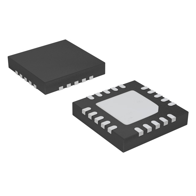
- Part No.:
- PTN5100BSMP
- Manufacturer:
- NXP Semiconductors
- Category:
- Controllers
- Package:
- 20-VFQFN Exposed Pad
- Datasheet:
-
 PTN5100BSMP.pdf
- Description:
- IC USB PD PHY TYPE C 20HVQFN
- Quantity:
- Payment:

- Shipping:

Inventory:4,463
Please send an inquiry. Send us your inquiry, and we will respond immediately.
Product details
Overview
PTN5100BSMP from NXP Semiconductors is a single-port USB Type-C Power Delivery PHY and Protocol IC that implements the physical layer (BMC/4B5B/CRC), protocol layer (packet assembly/disassembly, retries, resets), and Type-C configuration channel (CC1/CC2) functions for host or device-side PD implementations. It supports Provider (P), Consumer (C), and Dual-Role (P/C, C/P) operation with register- and NVM-programmable DFP/UFP/DRP roles, VCONN low-RON switching (1 A, 2.7–5.5 V), and operates from VDD (3.3 V ±10%) or VBUS (up to 25 V) - enabling Dead Battery mode in notebooks and Chromebooks.
For engineers reviewing the PTN5100BSMP datasheet, PTN5100BSMP pinout, PTN5100BSMP application, or PTN5100BSMP equivalent, key selection considerations include its dual SPI/I2C interface (pre-configured at factory), CC orientation detection via CC_ORIENT pin, programmable forward/reverse current protection on VCONN, open-drain FET enable outputs (EN_USBSRC/EN_USBFET1/EN_USBFET2), and HVQFN20 package compatibility with thermal pad grounding requirements.
Technical Context
PTN5100BSMP integrates a full USB PD PHY (slew-controlled BMC encoding/decoding, 4B5B line coding, CRC generation/checking) and protocol engine (SOP/SOP'/SOP'' handling, Good CRC response, automated retries, hard/cable reset management) tightly coupled with a Type-C CC block supporting Rp/Rd programmability, plug orientation detection, and debug accessory identification. Its autonomous CC front-end enables dead-battery UFP behavior without MCU intervention.
The IC features three open-drain gate drivers (EN_USBSRC, EN_USBFET1, EN_USBFET2) for external PMOS power path control, a 1 A VCONN switch with register-programmable forward/reverse current protection, and dual-domain power architecture: VDD/VIO for core/IO logic and VBUS for dead-battery operation. Interface selection (SPI or I2C) is factory-set via NVM; I2C supports three slave addresses (0xE0/0xE4/0xE8 write).
Key Specifications
| Parameter | Value and Actual Design Meaning |
|---|---|
| USB Compliance | Fully compliant with USB PD 2.0 and USB Type-C 1.2 specifications including delta updates. |
| Operating Voltage | VDD = 3.3 V ±10%; VBUS operational up to 25 V (tolerant to 28 V); enables Dead Battery operation when VDD is absent. |
| Interface Options | SPI slave (modes 1/2, up to 30 MHz) or I2C slave (100 kHz / 400 kHz / 1 MHz); factory pre-configured, not runtime-switchable. |
| VCONN Switch | Low-RON switch delivering up to 1 A from 2.7 V to 5.5 V; includes register-programmable forward and reverse current protection. |
| Temperature Range | −20 °C to +85 °C ambient operating range, qualified for industrial and computing platform use. |
| ESD Rating | 8 kV HBM, 1 kV CDM - meets robustness requirements for USB connector-facing ICs. |
| Package | HVQFN20 (4 mm × 4 mm, 0.5 mm pitch) with exposed thermal pad requiring PCB soldering and thermal vias. |
Pinout & Package
HVQFN20 package (SOT917-4) with 4 mm × 4 mm body, 0.5 mm pitch, and exposed center ground pad requiring direct soldering to PCB ground plane and thermal vias for reliable operation.
| Pin/Terminal | Circuit Role | Design Meaning |
|---|---|---|
| CC1 / CC2 | Type-C Configuration Channel I/O | Dual-purpose analog IO pins for Rp/Rd detection, cable connect/disconnect sensing, and orientation determination per USB Type-C spec. |
| CC_ORIENT | Cable Orientation Indicator | CMOS output on VIO rail indicating plug orientation (LOW = CC1 active, HIGH = CC2 active) after MCU initialization. |
| EN_USBSRC / EN_USBFET1 / EN_USBFET2 | PMOS Gate Enable Outputs | Open-drain outputs driving external VBUS source/sink FETs; Hi-Z at POR, driven LOW by PTN5100BSMP based on PD role and policy commands. |
| VCONN_IN | VCONN Power Input | Input pin accepting 2.7–5.5 V to power full-featured cables; enables VCONN switch only when within valid range. |
| SPI_CLK_I2C_SCL / SPI_MOSI_I2C_SDA / SPI_CS / SPI_MISO | Host Interface Signals | Dual-function pins supporting either SPI (push-pull CMOS) or I2C (open-drain) communication; interface mode fixed at factory. |
| INT_N | Interrupt Output | Active-low, level-triggered open-drain interrupt signaling CC events, VCONN faults, or PD protocol status changes to MCU. |
| V_MCUPWR | MCU Power Supply | Output delivering up to 30 mA to power external policy controller MCU; requires 2.2 µF decoupling capacitor. |
| SLV_ADDR | I2C Address Select | Ternary input setting I2C slave address to 0xE0, 0xE4, or 0xE8 (write) - enables up to three PTN5100BSMP devices on one bus. |
Key Features
| Feature | Design Value |
|---|---|
| Programmable Type-C Role | NVM- and register-configurable DFP/UFP/DRP operation with Rd/Rp pull-down/up behavior optimized for dead-battery platforms. |
| Robust VCONN Protection | Integrated forward current protection (trip threshold register-programmable) and reverse current protection to prevent inductive backfeed during cable unplug. |
| Autonomous CC Front-End | Hardware-accelerated CC state machine detecting plug orientation, debug accessories, and connection events without MCU polling. |
| Dual-Power Domain Support | Independent VDD (core) and VIO (IO) rails allow interfacing with systems using different IO voltage levels; VBUS-powered operation sustains functionality during dead battery. |
| Multi-Standard Interface | Single hardware supporting SPI (30 MHz) or I2C (1 MHz Fast Mode Plus); eliminates need for external level shifters or protocol translators. |
| System-Level FET Control | Three dedicated open-drain gate drivers coordinate VBUS source/sink paths per PD contract - simplifying power path design in multi-role ports. |
Applications
| Notebook PC Charging Port | USB-C Docking Station |
|---|---|
|
Use Scenario: A Windows notebook implements USB-C as its sole charging and peripheral interface, requiring seamless PD negotiation with adapters and docks while maintaining operation during battery depletion. IC Role / Device Role / Timing Role: PTN5100BSMP serves as the PD PHY/Protocol layer, handling BMC decoding, SOP packet exchange, and VCONN switching under control of the embedded controller. Use Value: Enables Dead Battery boot via VBUS-powered operation, supports DRP role switching between charger (P) and peripheral (C), and provides orientation-aware CC routing for stable link establishment. |
Use Scenario: A compact USB-C dock aggregates video (DP Alt Mode), data (USB 3.1), and power delivery (up to 100 W) while managing multiple upstream/downstream port roles. IC Role / Device Role / Timing Role: PTN5100BSMP acts as the Type-C CC and PD protocol engine for the dock's upstream-facing port (UFP), negotiating power contracts and detecting debug accessories. Use Value: Delivers precise Rp/Rd indication for accessory detection, generates SOP' packets for debug mode entry, and isolates VCONN current to prevent backfeed into the dock's power domain. |
| Chromebook Peripheral Hub | Smartphone Fast Charging Circuit |
|
Use Scenario: A low-power Chromebook hub adds HDMI, Ethernet, and SD card slots via USB-C, requiring minimal BOM count and guaranteed interoperability with certified chargers. IC Role / Device Role / Timing Role: PTN5100BSMP operates as a DFP-only PD controller, managing VBUS sourcing, CC orientation reporting, and power contract enforcement. Use Value: Reduces firmware complexity by offloading BMC timing and CRC validation to hardware, while open-drain FET enables direct drive of discrete power MOSFETs without level shifters. |
Use Scenario: A flagship smartphone uses USB-C for fast charging (PPS/EPR) and video output, demanding reliable cable detection and rapid PD contract renegotiation during mode switches. IC Role / Device Role / Timing Role: PTN5100BSMP functions as a C/P dual-role port controller, detecting plug orientation, enabling VCONN for active cables, and signaling DP Alt Mode readiness. Use Value: Provides sub-100 ms orientation detection via CC_ORIENT pin, supports SOP''-debug for vendor-specific commands, and maintains PD link stability during dynamic power profile changes. |
Equivalent & Alternatives
The following parts are listed as comparable options for similar USB Type-C PD PHY and protocol applications.
| Alternative Part | Technical Difference | Application Difference | Selection Advice |
|---|---|---|---|
| TI TUSB1146 | Single-port USB-C PD transceiver with integrated BMC codec and CC logic; lacks VCONN switch and FET gate drivers. | Requires external VCONN LDO and discrete FET control logic; suited for simpler DFP-only designs without sink capability. | Select when system already implements VCONN regulation and power path FETs separately; not drop-in for PTN5100BSMP's integrated gate drive. |
| STUSB4500 | USB-C PD controller with embedded ARM Cortex-M0+; integrates policy engine but no VCONN switch or FET drivers. | Self-contained solution for basic PD negotiation; cannot support complex DRP transitions or high-current VCONN loads without external components. | Choose for cost-sensitive, low-complexity C-only applications where MCU integration reduces BOM count; unsuitable for high-reliability VCONN-critical docks. |
Compared with TI TUSB1146 and STUSB4500, PTN5100BSMP uniquely combines full PD PHY/protocol offload, integrated 1 A VCONN switching with reverse current protection, and three dedicated open-drain FET gate drivers - enabling complete single-chip USB-C port control in resource-constrained computing platforms without external power path logic.
Availability
PTN5100BSMP is available at Aetrix Electronics and suitable for notebook PCs, USB-C docking stations, and Chromebook peripheral hubs requiring stable component supply, long-term lifecycle support, and compliance-certified USB Type-C PD implementation.
Supply support for PTN5100BSMP includes scheduled delivery planning, volume procurement assistance, BOM continuity management, traceable sourcing, and lifecycle availability coordination for OEM customers, industrial embedded developers, connected-device designers, and electronics production programs.
Manufacturer
NXP Semiconductors is a global semiconductor company specializing in secure connectivity solutions for automotive, industrial, and consumer electronics, with leadership in USB, NFC, and secure authentication technologies.
PTN5100BSMP belongs to NXP's USB Type-C Power Delivery PHY and Protocol IC product line, designed specifically to offload timing-critical PD physical and protocol layer functions from host MCUs in space-constrained computing platforms.
FAQ
What is the primary function of the PTN5100BSMP in a USB-C system?
The PTN5100BSMP serves as a dedicated USB Type-C Power Delivery PHY and Protocol IC, implementing the physical layer (BMC encoding/decoding, 4B5B line coding, CRC), protocol layer (SOP packet handling, retries, resets), and Type-C configuration channel (CC1/CC2) functions. It works alongside an external policy controller MCU to deliver full PD functionality while offloading timing-critical tasks - enabling robust, standards-compliant USB-C port implementation in notebooks, docks, and mobile devices. The PTN5100BSMP itself does not contain a policy engine.
Does PTN5100BSMP support Dead Battery operation, and how is it implemented?
Yes, PTN5100BSMP supports Dead Battery (DB) operation by drawing power directly from VBUS (up to 25 V) instead of VDD. When VDD is absent, the IC remains fully functional - maintaining CC detection, orientation reporting via CC_ORIENT, VCONN switching, and SPI/I2C communication - allowing the host system to boot and negotiate power contracts even with zero battery charge. This capability is critical for notebook and Chromebook platforms requiring guaranteed USB-C port responsiveness during DB conditions. The PTN5100BSMP handles VBUS-to-core power conversion internally.
How is the interface type (SPI vs. I2C) selected for PTN5100BSMP?
The interface type for PTN5100BSMP - SPI or I2C - is factory pre-configured in non-volatile memory (NVM) and cannot be changed in-system. The selection is fixed at manufacturing based on orderable part number: PTN5100BSMP is configured for SPI interface, while PTN5100ABSMP is configured for I2C. Both variants share identical pinout and functionality except for interface mode. Users must select the correct variant at procurement; no runtime reconfiguration or software toggle is supported. The PTN5100BSMP datasheet confirms SPI mode support up to 30 MHz.
What protection features does PTN5100BSMP provide on its CC and VBUS pins?
PTN5100BSMP provides 5.5 V tolerance on CC1 and CC2 pins, and 28 V tolerance on the VBUS pin and VBUS power path MOSFET enable pins (EN_USBSRC/EN_USBFET1/EN_USBFET2). It also includes back-current protection on all pins when unpowered, ensuring no leakage paths compromise system integrity during power sequencing. These ratings allow direct connection to USB-C connectors without external TVS diodes for basic ESD suppression - though NXP recommends PESD5V0S1USF-type protection for cable plug/unplug transients. All protection features are inherent to the PTN5100BSMP silicon design.
Can PTN5100BSMP operate as both a USB-C provider and consumer on the same port?
Yes, PTN5100BSMP supports Dual-Role Power (DRP) operation - functioning as either Provider (P), Consumer (C), or Provider/Consumer (P/C) on a single port - through NVM and register programming. Its DRP capability includes configurable Rp/Rd pull-up/down on CC pins, orientation-aware CC routing, and coordinated control of EN_USBSRC and EN_USBFET1/2 outputs to manage bidirectional VBUS power flow. This enables dynamic role swapping in devices like laptops and docks without hardware modification. The PTN5100BSMP implements the physical and protocol layers required for DRP; the policy decision logic resides in the external MCU.
PTN5100BSMP Specifications
- Product attributes
- Attribute value
- Manufacturer:
- NXP Semiconductors
- Package/Case:
- 20-VFQFN Exposed Pad
- Programmable:
- Not Verified
- Protocol:
- USB
- Function:
- Controller
- Interface:
- USB
- Standards:
- -
- Voltage - Supply:
- -
- Current - Supply:
- -
- Operating Temperature:
- -20°C ~ 85°C
- Supplier Device Package:
- 20-HVQFN (4x4)
- Grade:
- -
- Qualification:
- -
PTN5100BSMP FAQ
1.How can I place an order for PTN5100BSMP through Aetrix?
Please submit a Request for Quotation (RFQ) for PTN5100BSMP on Aetrix. Our sales agent will provide a competitive quotation and guide you through the order confirmation once you accept the terms.
2.Are the price and stock information for PTN5100BSMP reliable?
The price and inventory of PTN5100BSMP are updated periodically and may fluctuate due to market conditions. Stock and pricing data are typically refreshed every 24 hours. Quotation validity for PTN5100BSMP is usually 5 days.
3.What payment methods are accepted for PTN5100BSMP?
We accept Wire Transfer, PayPal, Credit Card, Western Union, MoneyGram, and Escrow for PTN5100BSMP transactions.
Note: Certain payment methods may incur a processing fee.
4.How is shipping managed for PTN5100BSMP?
PTN5100BSMP orders can be shipped via leading logistics carriers, including DHL, UPS, FedEx, TNT, or Registered Mail.
Once your PTN5100BSMP order is processed, you will receive an email with the shipment details and tracking number.
Note: Tracking information may take up to 24 hours to appear. Express delivery typically takes 3–5 business days.
5.How can I obtain technical support or documentation for PTN5100BSMP?
For technical support, including PTN5100BSMP datasheets, pinout diagrams, or application guidance, please contact our engineering support team. They can provide detailed documentation and assistance for your PTN5100BSMP requirements.
6.How does Aetrix verify that PTN5100BSMP is sourced from the original manufacturer or authorized distributors?
All PTN5100BSMP products on Aetrix are procured from qualified distributors and authorized channels. Our dedicated quality assurance team conducts strict verification, including traceability checks and, if necessary, third-party testing. This ensures that PTN5100BSMP meets industry standards.
7.What is the process for return or replacement of PTN5100BSMP?
All PTN5100BSMP units undergo pre-shipment inspection (PSI). If there is an issue with PTN5100BSMP, returns or replacements are accepted under the following conditions:
1.Quantity discrepancies, incorrect items, or visible external defects (such as breakage or corrosion), acknowledged by Aetrix.
2.The issue is reported within 90 days of delivery.
3.The PTN5100BSMP part is unused and in its original packaging.
Return procedure for PTN5100BSMP:
1.Submit a request within 90 days.
2.Obtain a Return Material Authorization (RMA) from Aetrix.
PTN5100BSMP Tags

-
PTN5150AHXMP
NXP Semiconductors

-
USB3740B-AI9-TR
Microchip Technology

-
USB3740B-AI2-TR
Microchip Technology

-
USB3300-EZK-TR
Microchip Technology
-
USB3300-EZK
Microchip Technology

-
FUSB340TMX
onsemi

-
FUSB302BMPX
onsemi

-
DP83826IRHBR
Texas Instruments

-
MCP2518FDT-E/QBB
Microchip Technology
-
FUSB302MPX
onsemi

-
MCP2518FDT-E/SL
Microchip Technology

-
FT260Q-R
FTDI, Future Technology Devices International Ltd
Tech Hub

A practical engineering guide to 3.3V and 5V logic compatibility, input thresholds, resistor dividers, translator ICs, MOSFET level shifting, I2C pull-ups, timing limits and power-sequencing risks.

The 74HC595 uses push-pull logic outputs, while the TPIC6B595 uses 50 V open-drain DMOS sinks for higher-power loads. This guide compares timing, current limits, 3.3 V interfacing, load wiring, thermal…

The 74HC595 converts serial data into eight stable parallel outputs. This guide covers pin functions, shift and storage timing, OE and MR behavior, drive-current limits, cascading, voltage compatibilit…

A technical comparison of level-sensitive latches and edge-triggered flip-flops, covering timing windows, setup and hold limits, master–slave operation, time borrowing, race-through, HDL inference and…

A D latch stores one bit while Enable controls when data can pass. This reference covers gate-level operation, truth tables, transparency, setup and hold timing, LE versus OE, common ICs and practical …

An SR latch stores one bit through cross-coupled feedback. This engineering reference covers NOR and NAND implementations, truth tables, forbidden-state recovery, gated operation, switch debouncing, fa…

Latch circuits retain one bit through feedback. This technical reference covers SR and D latches, truth tables, transparency, timing limits, latch-versus-flip-flop behavior, applications and common log…

An engineering guide to LED driver operation, constant-current and constant-voltage outputs, linear and switching topologies, dimming, IC selection, calculations, replacement compatibility, and fault c…

Operational amplifier guide covering op amp basics, feedback, ideal vs real op amps, common configurations, buffer circuits, offset, bias current, gain-bandwidth, slew rate, rail-to-rail limits and sel…

Jumper cables guide covering safe connection order, red and black clamp placement, final ground connection, cable gauge, length, clamp quality, copper vs CCA cables, jump starter comparison and battery…


