
 My Inquiry
 My Account


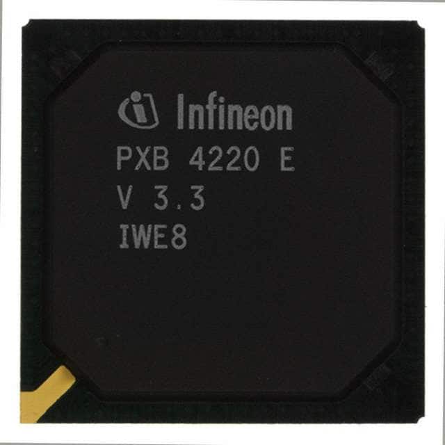
Infineon Technologies PXB 4221 E V3.4-G
- Part No.:
- PXB 4221 E V3.4-G
- Manufacturer:
- Infineon Technologies
- Category:
- Specialized ICs
- Package:
- 256-BGA
- Datasheet:
-
 PXB 4221 E V3.4-G.pdf
- Description:
- IC INTERWORKING ELEMENT 256BGA
- Quantity:
- Payment:

- Shipping:

Inventory:3,349
Please send an inquiry. Send us your inquiry, and we will respond immediately.
Product details
Overview
PXB 4221 E V3.4-G from Infineon Technologies is an Interworking Element (IWE8) IC designed for ATM and AAL5 segmentation/reassembly in multi-E1/T1 line cards, supporting up to 8 E1 or 8 T1 lines with integrated clock recovery, UTOPIA Level 2 interface, and IMA support. It delivers 8× E1/T1 framing, ATM cell delineation with HEC generation/check, CAS-aware structured CES, and fractional PLL-based clock synchronization.
For engineers reviewing the PXB 4221 E V3.4-G datasheet, PXB 4221 E V3.4-G pinout, PXB 4221 E V3.4-G application, or PXB 4221 E V3.4-G equivalent, this device serves as a core framer-to-ATM interworking engine in carrier-grade access equipment requiring precise timing alignment, echo cancellation integration, and deterministic cell transport across legacy TDM and ATM domains.
Technical Context
The PXB 4221E implements dual-path processing: one path handles generic framer interface (FALC/GIM/SYM/EC modes) for E1/T1 line termination, while the other executes ATM layer functions including cell scrambling/descrambling, HEC generation/correction, and OAM processing. Its internal clock recovery circuit (ICRC) supports SRTS, ACM, and FILTER PLL modes with fractional divider for jitter-tolerant synchronization to network-derived clocks.
It features dedicated hardware blocks for AAL5 segmentation (with RTS extraction, padding, and CAS conditioning) and reassembly (with sequence number protection, dummy cell insertion, and SDT-port synchronization), all managed via microprocessor interface and supported by external RAM for buffer storage. The UTOPIA Level 2 interface operates at 25 MHz with backpressure signaling for flow control.
Key Specifications
| Parameter | Value and Actual Design Meaning |
|---|---|
| E1/T1 Line Support | 8 independent E1 or T1 lines - enables full DS1/E1 line card consolidation without external multiplexing. |
| UTOPIA Interface | Level 2, 25 MHz - provides direct connection to ATM PHY or switch fabric with port-addressed cell transfer and backpressure signaling. |
| ATM Cell Rate | Up to OC-3 (155.52 Mbps) aggregate - supports full-rate transport of 8× E1 (8.448 Mbps) or 8× T1 (6.312 Mbps) over ATM. |
| Clock Recovery | Internal PLL with SRTS/ACM/FILTER modes and fractional divider - locks to recovered line timing with ±50 ppm holdover and sub-10 ns jitter accumulation. |
| AAL5 Handling | Hardware-accelerated segmentation & reassembly with RTS verification and CAS freezing - eliminates CPU overhead for voice/data CES transport. |
| Microprocessor Interface | 8-/16-bit parallel bus with interrupt and DMA-ready signals - enables real-time configuration and status monitoring in embedded control systems. |
| Power Supply | 3.3 V core / 2.5 V I/O - compatible with standard telecom logic rails and low-power line card designs. |
Pinout & Package
Package: 256-pin LQFP (28 mm × 28 mm, 0.4 mm pitch), RoHS-compliant, thermally enhanced for telecom line card operation.
| Pin/Terminal | Circuit Role | Design Meaning |
|---|---|---|
| CLKIN | Reference Clock Input | Accepts 2.048 MHz or 8.192 MHz system clock for frame synchronization and PLL reference. |
| CLKOUT | Recovered Clock Output | Provides jitter-filtered 2.048/8.192 MHz clock derived from line timing for downstream framer or codec use. |
| UTOPIA_CLK | UTOPIA Interface Clock | 25 MHz input driving UTOPIA data/strobe transfers; phase-aligned to ensure setup/hold compliance. |
| DATA[15:0] | Parallel Data Bus | 16-bit bidirectional bus for microprocessor register access and configuration memory mapping. |
| INT | Interrupt Request | Active-low asynchronous signal indicating event queue overflow, cell loss, or reassembly buffer underflow. |
| RESET_N | Asynchronous Reset | Active-low signal initializing all internal state machines, registers, and buffers to known power-on condition. |
Key Features
| Feature | Design Value |
|---|---|
| Integrated Clock Recovery (ICRC) | Eliminates need for external clock synthesizer or jitter cleaner in E1/T1-to-ATM gateways. |
| Hardware AAL5 Segmentation/Reassembly | Offloads CPU from CES payload handling, enabling real-time voice transport with <100 µs latency. |
| Multi-Mode Framer Interface | Supports FALC, GIM, SYM, and Echo Canceller modes on same pins - simplifies board design across E1/T1 variants. |
| UTOPIA Level 2 + Backpressure | Enables seamless integration with ATM PHYs and switches while preventing cell loss during congestion. |
| CAS-Aware Structured CES | Maintains channel-associated signaling integrity across ATM transport - essential for SS7 and ISDN applications. |
Applications
| DSLAM Line Card | VoIP Gateway |
|---|---|
|
Use Scenario: Aggregating 8 E1 lines from copper access networks into ATM backbone. IC Role / Device Role / Timing Role: Interworking Element converting TDM frames to ATM cells with SRTS-aligned clock recovery. Use Value: Enables carrier-grade timing traceability per ITU-T G.823/G.8261 while supporting legacy E1 service continuity. |
Use Scenario: Transporting T1-based PBX trunks over ATM infrastructure to centralized softswitches. IC Role / Device Role / Timing Role: ATM framer with CAS preservation and HEC correction for error-resilient voice transport. Use Value: Maintains DTMF, fax, and modem signal integrity across ATM segments without protocol conversion overhead. |
| IMA Concentrator | Cell-Based Echo Canceller Platform |
|
Use Scenario: Bundling multiple lower-speed E1 links into single high-bandwidth IMA group for backhaul. IC Role / Device Role / Timing Role: IMA interface controller with cell interleaving, delay compensation, and CRC-10 generation. Use Value: Achieves deterministic cell delay variation (CDV) < 25 µs across 8-link IMA groups per ITU-T I.363.5. |
Use Scenario: Hosting echo canceller algorithms on DSP alongside T1 line termination. IC Role / Device Role / Timing Role: Echo Canceller Mode (EC) interface providing synchronized sample streams and control signaling. Use Value: Enables tight coupling between line interface and DSP for <64 ms round-trip echo tail coverage with zero frame misalignment. |
Equivalent & Alternatives
The following parts are listed as comparable options for similar interworking element applications.
| Alternative Part | Technical Difference | Application Difference | Selection Advice |
|---|---|---|---|
| PMC-Sierra PM5352 (TIGER) | Single-chip ATM SAR with integrated UTOPIA and PCI interface; lacks native E1/T1 framer - requires external FALC. | Targeted at PCI-based ATM adapter cards, not line-card-integrated framer+SAR solutions. | Select when host interface is PCI and framer is already implemented externally. |
| Conexant CX82310 | Dual-E1 framer with basic ATM cell processing but no hardware AAL5 SAR or IMA support - limited to 2-line capacity. | Suitable for small-scale VoIP gateways, not carrier-class 8-line aggregation. | Select only for cost-sensitive, low-channel-count deployments where full IWE8 functionality is unnecessary. |
Compared with PM5352 and CX82310, the PXB 4221E uniquely integrates full 8-line E1/T1 framing, hardware AAL5 SAR, IMA, and clock recovery in one package - eliminating external framer, clock IC, and SAR accelerator components required by alternatives.
Availability
PXB 4221 E V3.4-G is available at Aetrix Electronics and suitable for DSLAM line cards, VoIP gateways, IMA concentrators, and echo canceller platforms requiring stable component supply and long-term lifecycle support in telecom infrastructure.
Supply support for PXB 4221 E V3.4-G includes scheduled delivery planning, volume procurement assistance, BOM continuity management, traceable sourcing, and lifecycle availability coordination for OEM customers, industrial embedded developers, connected-device designers, and electronics production programs.
Manufacturer
Infineon Technologies AG is a German semiconductor manufacturer specializing in power management, automotive, security, and communications ICs, with deep heritage in telecom silicon dating to Siemens' semiconductor division.
The PXB 4221E belongs to Infineon's IWE (Interworking Element) product line, engineered specifically for TDM-to-ATM interworking in carrier-access equipment where timing precision, protocol transparency, and hardware offload are critical.
FAQ
What clock sources does the PXB 4221E support for E1 line synchronization?
The PXB 4221E supports direct E1 line clock recovery via its internal Clock Recovery Circuit (ICRC), accepting 2.048 MHz or 8.192 MHz reference inputs. It implements SRTS, ACM, and FILTER PLL modes with fractional divider to lock onto network-derived timing with ±50 ppm tolerance and sub-10 ns jitter accumulation - meeting ITU-T G.823 requirements for primary rate interfaces.
Does the PXB 4221E support both structured and unstructured CES for voice transport?
Yes - the PXB 4221E supports both unstructured CES (bit-transparent transport) and structured CES with CAS (channel-associated signaling) preservation. In structured mode, it freezes CAS bits upstream during segmentation and reinserts them downstream during reassembly, maintaining compatibility with SS7, ISDN PRI, and legacy PBX signaling protocols without requiring external CAS processors.
Can the PXB 4221E operate in standalone mode without external microprocessor control?
No - the PXB 4221E requires initialization and runtime configuration via its 8-/16-bit microprocessor interface. All functional blocks (framer mode selection, ATM port setup, SAR channel mapping, PLL configuration) are register-controlled. While it executes segmentation/reassembly autonomously once configured, boot-up, fault handling, and dynamic reconfiguration depend on host processor interaction.
How does the PXB 4221E handle cell loss during reassembly?
Upon detecting missing cells (via sequence number gaps), the PXB 4221E inserts dummy cells into the reassembly buffer to maintain payload alignment and prevent downstream frame slips. This behavior is configurable per channel and complies with RFC 2680 for cell loss concealment in AAL5 CES applications, ensuring continuous voice stream delivery even under moderate packet loss conditions.
PXB 4221 E V3.4-G Specifications
- Product attributes
- Attribute value
- Manufacturer:
- Infineon Technologies
- Series:
- -
- Package/Case:
- 256-BGA
- Packaging:
- Tray
- Product Status:
- Obsolete
- Programmable:
- Not Verified
- Type:
- Interworking Element
- Applications:
- -
- Mounting Type:
- Surface Mount
- Supplier Device Package:
- PG-BGA-256-1
- Grade:
- -
- Qualification:
- -
PXB 4221 E V3.4-G FAQ
1.How can I place an order for PXB 4221 E V3.4-G through Aetrix?
Please submit a Request for Quotation (RFQ) for PXB 4221 E V3.4-G on Aetrix. Our sales agent will provide a competitive quotation and guide you through the order confirmation once you accept the terms.
2.Are the price and stock information for PXB 4221 E V3.4-G reliable?
The price and inventory of PXB 4221 E V3.4-G are updated periodically and may fluctuate due to market conditions. Stock and pricing data are typically refreshed every 24 hours. Quotation validity for PXB 4221 E V3.4-G is usually 5 days.
3.What payment methods are accepted for PXB 4221 E V3.4-G?
We accept Wire Transfer, PayPal, Credit Card, Western Union, MoneyGram, and Escrow for PXB 4221 E V3.4-G transactions.
Note: Certain payment methods may incur a processing fee.
4.How is shipping managed for PXB 4221 E V3.4-G?
PXB 4221 E V3.4-G orders can be shipped via leading logistics carriers, including DHL, UPS, FedEx, TNT, or Registered Mail.
Once your PXB 4221 E V3.4-G order is processed, you will receive an email with the shipment details and tracking number.
Note: Tracking information may take up to 24 hours to appear. Express delivery typically takes 3–5 business days.
5.How can I obtain technical support or documentation for PXB 4221 E V3.4-G?
For technical support, including PXB 4221 E V3.4-G datasheets, pinout diagrams, or application guidance, please contact our engineering support team. They can provide detailed documentation and assistance for your PXB 4221 E V3.4-G requirements.
6.How does Aetrix verify that PXB 4221 E V3.4-G is sourced from the original manufacturer or authorized distributors?
All PXB 4221 E V3.4-G products on Aetrix are procured from qualified distributors and authorized channels. Our dedicated quality assurance team conducts strict verification, including traceability checks and, if necessary, third-party testing. This ensures that PXB 4221 E V3.4-G meets industry standards.
7.What is the process for return or replacement of PXB 4221 E V3.4-G?
All PXB 4221 E V3.4-G units undergo pre-shipment inspection (PSI). If there is an issue with PXB 4221 E V3.4-G, returns or replacements are accepted under the following conditions:
1.Quantity discrepancies, incorrect items, or visible external defects (such as breakage or corrosion), acknowledged by Aetrix.
2.The issue is reported within 90 days of delivery.
3.The PXB 4221 E V3.4-G part is unused and in its original packaging.
Return procedure for PXB 4221 E V3.4-G:
1.Submit a request within 90 days.
2.Obtain a Return Material Authorization (RMA) from Aetrix.
PXB 4221 E V3.4-G Tags

-
CAP200DG-TL
Power Integrations
-
ATSHA204A-MAHDA-T
Microchip Technology

-
ATSHA204A-SSHDA-T
Microchip Technology

-
ATSHA204A-STUCZ-T
Microchip Technology
-
ATECC608B-MAHDA-T
Microchip Technology
-
ATECC608B-MAHCZ-S
Microchip Technology

-
ATECC608B-SSHDA-T
Microchip Technology
-
ATECC608B-MAHDA-S
Microchip Technology
-
ATECC608A-MAHDA-S
Microchip Technology
-
ATECC608B-MAVDA-T
Microchip Technology

-
ATECC608A-SSHDA-T
Microchip Technology
-
ATECC508A-MAHDA-T
Microchip Technology
Tech Hub

Operational amplifier guide covering op amp basics, feedback, ideal vs real op amps, common configurations, buffer circuits, offset, bias current, gain-bandwidth, slew rate, rail-to-rail limits and sel…

Jumper cables guide covering safe connection order, red and black clamp placement, final ground connection, cable gauge, length, clamp quality, copper vs CCA cables, jump starter comparison and battery…

LDO regulator guide covering low dropout voltage, power dissipation, thermal design, PSRR, output noise, capacitor stability, adjustable LDO circuits, LDO vs buck converter and datasheet selection chec…

Conditional Access Module guide covering CAM meaning, CI/CI+ interface, smart card authorization, DVB security workflow, TV and set-top box compatibility, internal electronics, ESD protection, connecto…

Guide to electronic component obsolescence covering EOL risk, PCN/PDN notices, last-time buy planning, replacement options, form-fit-function validation, counterfeit risk and BOM lifecycle management.

18650 battery guide covering lithium-ion cell basics, 3.6V/3.7V voltage, 4.2V charging, mAh and Wh capacity, protected cells, chargers, BMS, series-parallel packs, holders, welding and sourcing checks.…

Hall effect sensor guide covering working principle, linear and digital sensors, Arduino circuits, current sensing, speed detection, automotive applications, A3144 examples, signal filtering and datash…

Product Change Notification guide for electronic components, covering PCN meaning, PCN vs PDN/EOL, common change types, risk levels, form-fit-function review, engineering validation, BOM control, LTB/L…

A practical guide to blend door actuators, covering HVAC function, symptoms, location, AC and heater issues, reset and calibration, replacement cost, electrical diagnosis, compatibility checks, and rep…

Engineering guide to Raspberry Pi alternatives, covering chip-level differences, Orange Pi, ROCK, Jetson, Banana Pi, NanoPi, Compute Module, Pico, GPIO, camera, HAT compatibility, and replacement risks…


