
 My Inquiry
 My Account


Renesas QLX4600SIQT7
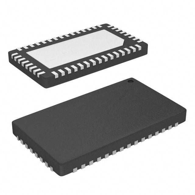
- Part No.:
- QLX4600SIQT7
- Manufacturer:
- Renesas
- Category:
- Specialized
- Package:
- 46-WFQFN Exposed Pad
- Datasheet:
-
 QLX4600SIQT7.pdf
- Description:
- IC INTERFACE SPECIALIZED 46TQFN
- Quantity:
- Payment:

- Shipping:

Inventory:760
Please send an inquiry. Send us your inquiry, and we will respond immediately.
Product details
Overview
QLX4600SIQT7 from Intersil (now Renesas) is a quad-channel receive-side equalizer IC for high-speed serial links, supporting up to 6.25 Gb/s line rates with CML I/O, 32-level programmable per-channel equalization, 30 m reach on 24 AWG twin-axial cable, and individual channel power-down for PCIe applications.
For engineers reviewing the QLX4600SIQT7 datasheet, QLX4600SIQT7 pinout, QLX4600SIQT7 application, or QLX4600SIQT7 equivalent, this device delivers deterministic signal restoration in DisplayPort v1.2, InfiniBand SDR/DDR, PCI Express Gen 1/2, and 10GBase-CX4 active cable assemblies - with no adaptation latency, full protocol-aware line silence preservation, and dual control modes (pin-selectable or serial bus).
Technical Context
The QLX4600SIQT7 implements four independent Current Mode Logic (CML) receive channels, each featuring a fixed-coefficient, non-adaptive equalizer followed by a limiting amplifier. Its architecture avoids closed-loop adaptation, enabling immediate signal fidelity restoration from the first bit at data rates from 2.5 to 6.25 Gb/s.
Each channel supports dual configuration paths: three CMOS control pins (CP[k][A,B,C]) for 18 discrete boost levels, or a 4-wire serial interface (DI/DO/CLK/ENB) for full 32-level register-based programming. Input impedance can be switched between 50 Ω (active) and >200 kΩ (power-down) via dedicated IS[k] pins, directly supporting PCIe Fundamental Reset signaling.
Key Specifications
| Parameter | Value and Actual Design Meaning |
|---|---|
| Data Rate | Up to 6.25 Gb/s NRZ - supports full-speed operation for DisplayPort HBR2, PCIe Gen2, and 10GBase-CX4 without derating. |
| Equalization Levels | 32 programmable settings via serial bus; 18 via control pins - enables precise per-channel compensation for varying cable gauges and lengths. |
| Power Consumption | 78 mW per channel (312 mW total) at 1.2 V - enables thermal feasibility in dense active cable modules and board-edge applications. |
| Propagation Delay | 500 ps max - ensures tight inter-lane timing alignment critical for multi-lane protocols like XAUI and SAS. |
| Cable Reach | 30 m on 24 AWG twin-axial cable - extends usable length beyond standard passive copper limits while maintaining BER integrity. |
| Output Residual Jitter | 0.25–0.35 UI at 6.25 Gb/s - meets jitter budget requirements for receiver input compliance in high-speed serial standards. |
| Line Silence Preservation | Active muting with <20 mVP-P output during electrical idle - maintains InfiniBand quiescent state and PCIe Electrical Idle Exit sequence integrity. |
Pinout & Package
QLX4600SIQT7 is housed in a RoHS-compliant 46-lead TQFN package (4 mm × 7 mm, 0.4 mm pitch) with exposed thermal pad. Pin assignments are validated per FN6979 Rev 2.00 datasheet, Page 3–4.
| Pin/Terminal | Circuit Role | Design Meaning |
|---|---|---|
| IN1[P], IN1[N] – IN4[P], IN4[N] | Differential CML inputs (4 channels) | Accept attenuated high-speed signals; require 100 nF low-ESL/ESR MLCC AC coupling per pair. |
| OUT1[P], OUT1[N] – OUT4[P], OUT4[N] | Differential CML outputs (4 channels) | Deliver restored 450–650 mVP-P swing into 50 Ω loads; support fast transition times (30–80 ps). |
| IS1–IS4 | CMOS channel power-down controls | Drive LOW to disable channel (input Z >200 kΩ, current drops to 3.8 mA), enabling PCIe link management. |
| CP1[A–C] – CP4[A–C] | 3-bit boost level select (per channel) | Set 18 discrete equalization levels via resistor-divider voltage; internally pulled down (25 kΩ). |
| DI, DO, CLK, ENB, MODE | Serial programming interface | Enable full 32-level register-based configuration; daisy-chainable across multiple devices. |
| DT | Detection Threshold reference | Sets LOS activation threshold; tie to GND to disable line silence preservation. |
| VDD (pins 4,7,10,29,32,35) | 1.2 V supply inputs | Require local 100 pF + 10 nF decoupling per pin for broadband noise suppression. |
| EXPOSED PAD | Thermal & electrical ground | Must be soldered to PCB ground plane for thermal dissipation (θJC = 2.3°C/W) and signal integrity. |
Key Features
| Feature | Design Value |
|---|---|
| No-adaptation equalization | Fixed-coefficient filter restores signal from first bit - eliminates convergence delay and pattern-dependent instability seen in adaptive equalizers. |
| Protocol-aware line silence | Mutes output to <20 mVP-P during electrical idle while preserving common-mode voltage - essential for InfiniBand and PCIe OOB signaling. |
| Per-channel power-down | Reduces channel current from 50 mA to 3.8 mA via IS[k] pins - enables dynamic power scaling in multi-lane systems. |
| Dual configuration interface | Supports both hardware-defined (CP pins) and firmware-controlled (serial bus) boost selection - balances layout simplicity with field-programmability. |
| Low-latency signal path | 500 ps propagation delay with <500 ps total latency - preserves inter-symbol timing margins in multi-gigabit links. |
Applications
| DisplayPort v1.2 Active Cable Module | InfiniBand SDR/DDR Interconnect |
|---|---|
Use Scenario: Extending DisplayPort source-to-display distance beyond 2 m using 24 AWG twin-axial cable in thin-profile docking stations. IC Role / Device Role / Timing Role: Receive-side equalizer restoring high-frequency content lost over copper; preserves HBR2 (5.4 Gb/s per lane) eye opening. Use Value: Enables 30 m reach at full bandwidth while maintaining <0.35 UI residual jitter - eliminating need for repeaters or optical conversion. |
Use Scenario: Building high-density InfiniBand leaf-spine switch interconnects with active copper cables in HPC clusters. IC Role / Device Role / Timing Role: Quad-channel lane extender compensating for skin/dielectric loss in long twin-axial runs; preserves quiescent state for link training. Use Value: Supports SDR (2.5 Gb/s) and DDR (5 Gb/s) modes with deterministic latency and guaranteed line silence - critical for reliable link initialization. |
| PCI Express Gen 2 Backplane Interface | 10GBase-CX4 Data Center Cabling |
Use Scenario: Enabling PCIe Gen2 (5 Gb/s) connectivity across backplane traces or mid-plane connectors in ATCA blade servers. IC Role / Device Role / Timing Role: Per-lane equalizer with IS[k]-controlled power-down during Fundamental Reset - synchronizes with PCIe link state machine. Use Value: Reduces per-lane power to 3.8 mA in L0s/L1 states while retaining fast wake-up (<20 ns response to ALIGN(0)) - improves system-level power efficiency. |
Use Scenario: Implementing cost-effective 10G Ethernet inter-rack cabling using active twin-axial assemblies instead of fiber. IC Role / Device Role / Timing Role: Quad-channel signal conditioner restoring 10GBase-CX4's 3.125 Gb/s lanes after 15+ meter channel loss. Use Value: Achieves BER <10−12 at 30 m on 24 AWG cable - replaces more expensive optical transceivers in short-reach data center topologies. |
Equivalent & Alternatives
The following parts are listed as comparable options for similar quad-channel receive equalizer applications.
| Alternative Part | Technical Difference | Application Difference | Selection Advice |
|---|---|---|---|
| ISL36411 | Higher 11 Gb/s data rate; 30 dB equalization; no line silence preservation; 440 mW total power. | Targeted at DP1.3 and 40GbE QSFP+ modules - lacks protocol-aware muting required for PCIe/InfiniBand. | Select ISL36411 only when >6.25 Gb/s operation is mandatory and line silence preservation is not required. |
| QLX4600-SL30 | Same 6.25 Gb/s rate and 30 m reach; uses 4-pin LOS detection instead of DT pin; identical power and package. | Optimized for SAS-6Gb and PCIe 2.0 where loss-of-signal flagging is prioritized over flexible threshold tuning. | Choose QLX4600-SL30 if system requires standardized LOS signaling rather than user-adjustable DT threshold. |
Compared with ISL36411 and QLX4600-SL30, QLX4600SIQT7 uniquely balances protocol-aware line silence, flexible DT threshold control, and PCIe-compatible power-down - making it the optimal choice for multi-standard active cable designs requiring interoperability across DisplayPort, InfiniBand, and PCIe.
Availability
QLX4600SIQT7 is available at Aetrix Electronics and suitable for DisplayPort v1.2 active cable modules, InfiniBand SDR/DDR interconnects, and 10GBase-CX4 data center cabling requiring stable component supply, long-term lifecycle support, and traceable sourcing.
Supply support for QLX4600SIQT7 includes scheduled delivery planning, volume procurement assistance, BOM continuity management, traceable sourcing, and lifecycle availability coordination for OEM customers, industrial embedded developers, connected-device designers, and electronics production programs.
Manufacturer
Renesas Electronics (formerly Intersil) is a global semiconductor leader specializing in analog, mixed-signal, and power management ICs for high-performance computing, communications, and industrial systems.
The QLX4600-S30 product line was designed specifically for high-density, low-power quad-lane extension in active copper cable assemblies - targeting DisplayPort, PCIe, and InfiniBand ecosystems with deterministic equalization and protocol-aware signal integrity.
FAQ
What is the maximum supported data rate for QLX4600SIQT7?
The QLX4600SIQT7 supports line rates up to 6.25 Gb/s NRZ, fully compliant with DisplayPort v1.2 HBR2, PCI Express Gen 2, InfiniBand DDR, and 10GBase-CX4. It also operates reliably at lower rates including 2.5, 3.125, 4.25, and 5 Gb/s - with consistent equalization performance across the entire range.
Does QLX4600SIQT7 support line silence preservation for InfiniBand and PCIe protocols?
Yes, QLX4600SIQT7 actively preserves line silence (electrical idle) by muting its differential outputs to <20 mVP-P when input amplitude falls below the DT pin threshold. This maintains InfiniBand quiescent state and PCIe Electrical Idle Exit sequence integrity - a key differentiator versus conventional limiting amplifiers.
How many equalization levels does QLX4600SIQT7 offer, and how are they configured?
QLX4600SIQT7 provides 32 equalization levels per channel when programmed via its serial interface (DI/DO/CLK/ENB), or 18 levels when set using external CP[k][A,B,C] control pins. The serial mode enables full flexibility and daisy-chaining; the pin mode offers board-level simplicity with no host controller dependency.
What is the power consumption of QLX4600SIQT7 per channel and in total?
QLX4600SIQT7 consumes 78 mW per channel under typical operation at 1.2 V, totaling 312 mW for all four channels. When a channel is powered down via its IS[k] pin, current draw drops from 50 mA to 3.8 mA - reducing per-channel power to ~4.6 mW and enabling dynamic power optimization in multi-lane systems.
What package type and thermal characteristics does QLX4600SIQT7 use?
QLX4600SIQT7 uses a 46-lead TQFN package (4 mm × 7 mm, 0.4 mm pitch) with exposed thermal pad. Its thermal resistance is θJA = 32°C/W and θJC = 2.3°C/W. The exposed pad must be soldered to the PCB ground plane to ensure proper thermal dissipation and maintain junction temperature ≤125°C under full-load conditions.
QLX4600SIQT7 Specifications
- Product attributes
- Attribute value
- Manufacturer:
- Renesas
- Series:
- QLx™
- Package/Case:
- 46-WFQFN Exposed Pad
- Packaging:
- Tape & Reel (TR)
- Product Status:
- Active
- Applications:
- Copper Cable Modules
- Interface:
- -
- Voltage - Supply:
- 1.1V ~ 1.3V
- Supplier Device Package:
- 46-TQFN (4x7)
- Grade:
- -
- Qualification:
- -
- Mounting Type:
- Surface Mount
QLX4600SIQT7 FAQ
1.How can I place an order for QLX4600SIQT7 through Aetrix?
Please submit a Request for Quotation (RFQ) for QLX4600SIQT7 on Aetrix. Our sales agent will provide a competitive quotation and guide you through the order confirmation once you accept the terms.
2.Are the price and stock information for QLX4600SIQT7 reliable?
The price and inventory of QLX4600SIQT7 are updated periodically and may fluctuate due to market conditions. Stock and pricing data are typically refreshed every 24 hours. Quotation validity for QLX4600SIQT7 is usually 5 days.
3.What payment methods are accepted for QLX4600SIQT7?
We accept Wire Transfer, PayPal, Credit Card, Western Union, MoneyGram, and Escrow for QLX4600SIQT7 transactions.
Note: Certain payment methods may incur a processing fee.
4.How is shipping managed for QLX4600SIQT7?
QLX4600SIQT7 orders can be shipped via leading logistics carriers, including DHL, UPS, FedEx, TNT, or Registered Mail.
Once your QLX4600SIQT7 order is processed, you will receive an email with the shipment details and tracking number.
Note: Tracking information may take up to 24 hours to appear. Express delivery typically takes 3–5 business days.
5.How can I obtain technical support or documentation for QLX4600SIQT7?
For technical support, including QLX4600SIQT7 datasheets, pinout diagrams, or application guidance, please contact our engineering support team. They can provide detailed documentation and assistance for your QLX4600SIQT7 requirements.
6.How does Aetrix verify that QLX4600SIQT7 is sourced from the original manufacturer or authorized distributors?
All QLX4600SIQT7 products on Aetrix are procured from qualified distributors and authorized channels. Our dedicated quality assurance team conducts strict verification, including traceability checks and, if necessary, third-party testing. This ensures that QLX4600SIQT7 meets industry standards.
7.What is the process for return or replacement of QLX4600SIQT7?
All QLX4600SIQT7 units undergo pre-shipment inspection (PSI). If there is an issue with QLX4600SIQT7, returns or replacements are accepted under the following conditions:
1.Quantity discrepancies, incorrect items, or visible external defects (such as breakage or corrosion), acknowledged by Aetrix.
2.The issue is reported within 90 days of delivery.
3.The QLX4600SIQT7 part is unused and in its original packaging.
Return procedure for QLX4600SIQT7:
1.Submit a request within 90 days.
2.Obtain a Return Material Authorization (RMA) from Aetrix.
QLX4600SIQT7 Tags

-
NVT4857UKAZ
NXP Semiconductors

-
TCA8418RTWR
Texas Instruments

-
PCA9546APWR
Texas Instruments

-
MD0100N8-G
Microchip Technology

-
PCA9548APW,118
NXP Semiconductors

-
PCA9540BDP,118
NXP Semiconductors

-
PCA9548APWR
Texas Instruments

-
PCA9546APW,118
NXP Semiconductors

-
PTN3360DBS,518
NXP Semiconductors

-
PCA9546ABS,118
NXP Semiconductors

-
PCA9518PWR
Texas Instruments

-
PCA9545APW,118
NXP Semiconductors
Tech Hub

TTL and CMOS logic families differ in thresholds, loading, output drive, power and timing. This engineering guide compares 74HC and 74HCT, calculates noise margins and checks 3.3 V/5 V compatibility.

A practical engineering guide to 3.3V and 5V logic compatibility, input thresholds, resistor dividers, translator ICs, MOSFET level shifting, I2C pull-ups, timing limits and power-sequencing risks.

The 74HC595 uses push-pull logic outputs, while the TPIC6B595 uses 50 V open-drain DMOS sinks for higher-power loads. This guide compares timing, current limits, 3.3 V interfacing, load wiring, thermal…

The 74HC595 converts serial data into eight stable parallel outputs. This guide covers pin functions, shift and storage timing, OE and MR behavior, drive-current limits, cascading, voltage compatibilit…

A technical comparison of level-sensitive latches and edge-triggered flip-flops, covering timing windows, setup and hold limits, master–slave operation, time borrowing, race-through, HDL inference and…

A D latch stores one bit while Enable controls when data can pass. This reference covers gate-level operation, truth tables, transparency, setup and hold timing, LE versus OE, common ICs and practical …

An SR latch stores one bit through cross-coupled feedback. This engineering reference covers NOR and NAND implementations, truth tables, forbidden-state recovery, gated operation, switch debouncing, fa…

Latch circuits retain one bit through feedback. This technical reference covers SR and D latches, truth tables, transparency, timing limits, latch-versus-flip-flop behavior, applications and common log…

An engineering guide to LED driver operation, constant-current and constant-voltage outputs, linear and switching topologies, dimming, IC selection, calculations, replacement compatibility, and fault c…

Operational amplifier guide covering op amp basics, feedback, ideal vs real op amps, common configurations, buffer circuits, offset, bias current, gain-bandwidth, slew rate, rail-to-rail limits and sel…


