
 My Inquiry
 My Account


NXP Semiconductors QN9090-001-T10
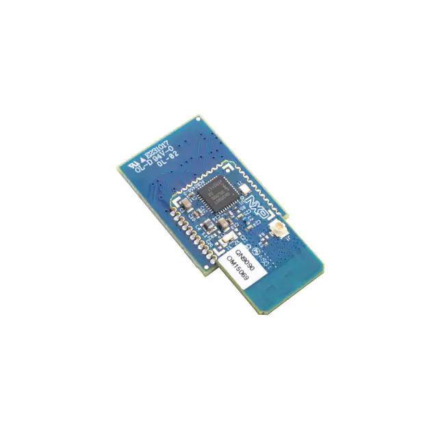
- Part No.:
- QN9090-001-T10
- Manufacturer:
- NXP Semiconductors
- Category:
- RF, RFID, Wireless Evaluation Boards
- Package:
- Datasheet:
-
 QN9090-001-T10.pdf
- Description:
- QN9090 BLE SOC DEV KIT
- Quantity:
- Payment:

- Shipping:

Inventory:1,484
Please send an inquiry. Send us your inquiry, and we will respond immediately.
Product details
Overview
QN9090-001-T10 from NXP is a Bluetooth 5.0 System-on-Chip module with integrated Arm® Cortex®-M4 CPU (48 MHz), 640 KB flash, 152 KB SRAM, and optional NFC Forum Type 2 Tag functionality - designed for ultra-low-power wearable and healthcare devices requiring robust -97 dBm RX sensitivity and +11 dBm TX output power.
For engineers reviewing the QN9090-001-T10 datasheet, QN9090-001-T10 pinout, QN9090-001-T10 application, or QN9090-001-T10 equivalent, key selection criteria include BLE 5.0 2 Mbps PHY support, integrated DC/DC converter, PDM-based voice activity detection, ISO7816 interface, and mezzanine-module form factor with pre-certified RF layout.
Technical Context
The QN9090-001-T10 implements a dual-mode BLE 5.0 transceiver with antenna diversity support and integrates an Arm Cortex-M4 core with Memory Protection Unit (MPU), enabling secure concurrent execution of BLE stack and application firmware. It includes dedicated hardware accelerators for AES-128/256, SHA-256, and true random number generation.
Its system architecture features a quad-SPI flash interface (SPIFI), two low-power wake-up timers, real-time clock, battery and temperature sensors, and a 12-bit 8-channel ADC - all managed via a centralized power management controller supporting multiple sleep modes with sub-μA retention current.
Key Specifications
| Parameter | Value and Actual Design Meaning |
|---|---|
| BLE Version | Bluetooth 5.0 compliant with 2 Mbps PHY - enables double data throughput vs BLE 4.2, reducing active time and average power consumption. |
| RX Sensitivity | -97 dBm at 1 Mbps - ensures reliable link budget in compact enclosures with marginal antenna efficiency. |
| TX Output Power | +11 dBm maximum - supports extended-range beaconing and sensor network deployment without external PA. |
| CPU Core | Arm Cortex-M4 @ 48 MHz with MPU - delivers deterministic real-time performance for concurrent BLE GATT services and sensor fusion algorithms. |
| Memory | 640 KB flash / 152 KB SRAM - accommodates full BLE stack, OTA update partition, and feature-rich application code with safe rollback. |
| NFC Interface | NFC Forum Type 2 Tag with 1912-byte EEPROM and 7-byte UID - enables touch-to-pair provisioning and unpowered device commissioning. |
| Operating Temp | -40°C to +125°C - validated for use in automotive cabin modules and industrial edge nodes without thermal derating. |
Pinout & Package
QN9090-001-T10 is a mezzanine-style module based on the QN9090T SoC in 40-pin HVQFN (6 mm × 6 mm, 0.85 mm height). The module integrates matching network, balun, and PCB trace antenna - pinout follows the underlying QN9090T die mapping with dedicated VBAT, VDD_IO, VDD_CORE, and RF_OUT pins routed to edge connectors.
| Pin/Terminal | Circuit Role | Design Meaning |
|---|---|---|
| VDD_CORE | Core supply rail | 1.1 V regulated input for Cortex-M4 and digital logic - requires local 1 μF ceramic decoupling. |
| VDD_IO | I/O supply rail | 1.8–3.6 V tolerant - powers GPIO, UART, I²C, and ADC reference; supports mixed-voltage interfacing. |
| RF_OUT | Transceiver RF output | Differential 50 Ω output feeding integrated balun - connects directly to PCB antenna or external RF switch. |
| NFC_SDA/NFC_SCL | NFC I²C interface | Open-drain signals compliant with NFC Forum Type 2 Tag spec - enable passive tap-to-pair without host CPU involvement. |
| PDM_CLK/PDM_DATA | Digital microphone interface | Supports PDM microphones for always-on voice activity detection - offloads audio preprocessing from CPU. |
Key Features
| Feature | Design Value |
|---|---|
| Integrated DC/DC Converter | Replaces external LDOs - reduces system BOM count and improves efficiency across 1.8–3.6 V input range. |
| Dedicated PDM Subsystem | Hardware-accelerated voice activity detection - enables wake-on-voice without CPU wake-up, extending battery life in wearables. |
| ISO7816 Interface | Smart card protocol support - allows secure credential storage and authentication in healthcare and access control applications. |
| Hardware Crypto Engine | AES-128/256 + SHA-256 acceleration - enables fast encrypted OTA updates and secure BLE pairing without software overhead. |
| Multi-Protocol Scalability | Pin-compatible with JN5189 and K32W041 families - permits firmware-only migration to IEEE 802.15.4 or Thread without PCB redesign. |
Applications
| Wearable Health Monitor | Sports Fitness Tracker |
|---|---|
Use Scenario: Continuous heart rate and SpO₂ monitoring in wrist-worn form factor with weekly battery life. IC Role / Device Role / Timing Role: BLE 5.0 SoC managing sensor acquisition, signal processing, and encrypted GATT-based data streaming to smartphone. Use Value: Ultra-low 4.3 mA RX peak current and -97 dBm sensitivity maintain connection through fabric and body attenuation. | Use Scenario: GPS-synchronized activity logging with motion fusion and real-time coaching feedback. IC Role / Device Role / Timing Role: Central controller executing sensor fusion algorithms while maintaining concurrent BLE connections to phone and peripheral sensors. Use Value: 640 KB flash reserves space for multi-sensor calibration tables and over-the-air firmware updates without compromising runtime memory. |
| Smart Home Beacon | HID Remote Control |
Use Scenario: Battery-powered retail or building automation beacon broadcasting Eddystone-URL with location context. IC Role / Device Role / Timing Role: Standalone BLE advertiser with RTC-triggered broadcast intervals and temperature-compensated timing. Use Value: +11 dBm TX output extends beacon range to 50+ meters in open indoor environments, reducing infrastructure density. | Use Scenario: Low-latency wireless remote for gaming peripherals or media controllers with tactile button response. IC Role / Device Role / Timing Role: HID-over-GATT endpoint with optimized connection interval handling and ISOchronous data channel support. Use Value: 2 Mbps PHY cuts report latency by 50% vs BLE 4.2 - critical for frame-accurate gaming input synchronization. |
Equivalent & Alternatives
The following parts are listed as comparable options for similar Bluetooth 5.0 SoC applications.
| Alternative Part | Technical Difference | Application Difference | Selection Advice |
|---|---|---|---|
| QN9090T | Same SoC die, bare-die HVQFN package (no integrated antenna or RF matching) | Requires custom RF layout and antenna integration - suitable for high-volume OEM designs with RF engineering resources | Select QN9090T when full RF optimization and mechanical integration flexibility are required. |
| nRF52840 DK | Arm Cortex-M4 @ 64 MHz, 1 MB flash, no integrated NFC tag or ISO7816 interface | Lacks out-of-band pairing capability and smart-card security interface - better suited for pure BLE mesh or USB-connected applications | Choose nRF52840 DK if NFC provisioning and contactless credentialing are not required. |
Compared with QN9090-001-T10, the QN9090T offers identical core functionality but demands RF design validation, while the nRF52840 DK provides higher clock speed and flash but omits NFC and ISO7816 - making QN9090-001-T10 optimal for certified, NFC-enabled, secure edge node deployments.
Availability
QN9090-001-T10 is available at Aetrix Electronics and suitable for wearable health monitors, sports fitness trackers, smart home beacons, and HID remote controls requiring stable component supply and pre-validated RF performance.
Supply support for QN9090-001-T10 includes scheduled delivery planning, volume procurement assistance, BOM continuity management, traceable sourcing, and lifecycle availability coordination for OEM customers, industrial embedded developers, connected-device designers, and electronics production programs.
Manufacturer
NXP Semiconductors is a global semiconductor company headquartered in Eindhoven, Netherlands, specializing in secure connectivity solutions for automotive, industrial, and IoT markets.
QN9090-001-T10 belongs to NXP's QN series of intelligent Bluetooth LE SoCs - engineered specifically for battery-constrained, NFC-enhanced edge devices demanding simultaneous processing, sensing, and secure wireless communication.
FAQ
What is the RF certification status of the QN9090-001-T10 module?
QN9090-001-T10 is a pre-certified module with FCC ID 2AJ8M-QN9090T10, IC 4112A-QN9090T10, CE RED, and RCM compliance. Its integrated antenna and matching network eliminate the need for end-product RF re-certification - significantly accelerating time-to-market for wearable and medical devices using QN9090-001-T10.
Does QN9090-001-T10 support Over-the-Air (OTA) firmware updates?
Yes, QN9090-001-T10 supports secure OTA updates via its 640 KB flash memory architecture, which includes dedicated bootloader and dual-bank update partitions. The hardware AES-256 engine encrypts update payloads, and the MCUXpresso SDK provides production-ready OTA example applications - ensuring robust field upgrades for QN9090-001-T10-based products.
Can QN9090-001-T10 operate without external crystal oscillators?
QN9090-001-T10 integrates both a 32 MHz crystal oscillator circuit and a 32.768 kHz free-running oscillator, but requires external 32 MHz and 32.768 kHz crystals for full BLE 5.0 timing accuracy and low-power RTC operation. The internal RC oscillators are not qualified for BLE radio timing - so external crystals remain mandatory for QN9090-001-T10 compliance.
How does the NFC capability of QN9090-001-T10 function during battery depletion?
The NFC Forum Type 2 Tag in QN9090-001-T10 operates passively using energy harvested from the NFC reader's RF field - meaning it remains functional even when the main battery is fully depleted. This enables device commissioning, diagnostics, and firmware recovery for QN9090-001-T10 throughout its entire lifecycle, including end-of-life servicing.
Is the QN9090-001-T10 module compatible with standard mezzanine carrier boards?
QN9090-001-T10 uses a standardized 2×15-pin 0.8 mm pitch mezzanine connector footprint aligned with NXP's reference carrier layouts. It is mechanically and electrically compatible with OM15080-QN9090 USB dongle baseboards and QN9090DK development platforms - allowing rapid prototyping and reuse of existing carrier infrastructure for QN9090-001-T10 integration.
QN9090-001-T10 Specifications
- Product attributes
- Attribute value
- Manufacturer:
- NXP Semiconductors
- Series:
- -
- Packaging:
- Bulk
- Product Status:
- Active
- Type:
- Transceiver; Bluetooth® 5.x (BLE)
- Frequency:
- 2.4GHz
- Contents:
- Board(s)
- Utilized IC / Part:
- QN9090
QN9090-001-T10 FAQ
1.How can I place an order for QN9090-001-T10 through Aetrix?
Please submit a Request for Quotation (RFQ) for QN9090-001-T10 on Aetrix. Our sales agent will provide a competitive quotation and guide you through the order confirmation once you accept the terms.
2.Are the price and stock information for QN9090-001-T10 reliable?
The price and inventory of QN9090-001-T10 are updated periodically and may fluctuate due to market conditions. Stock and pricing data are typically refreshed every 24 hours. Quotation validity for QN9090-001-T10 is usually 5 days.
3.What payment methods are accepted for QN9090-001-T10?
We accept Wire Transfer, PayPal, Credit Card, Western Union, MoneyGram, and Escrow for QN9090-001-T10 transactions.
Note: Certain payment methods may incur a processing fee.
4.How is shipping managed for QN9090-001-T10?
QN9090-001-T10 orders can be shipped via leading logistics carriers, including DHL, UPS, FedEx, TNT, or Registered Mail.
Once your QN9090-001-T10 order is processed, you will receive an email with the shipment details and tracking number.
Note: Tracking information may take up to 24 hours to appear. Express delivery typically takes 3–5 business days.
5.How can I obtain technical support or documentation for QN9090-001-T10?
For technical support, including QN9090-001-T10 datasheets, pinout diagrams, or application guidance, please contact our engineering support team. They can provide detailed documentation and assistance for your QN9090-001-T10 requirements.
6.How does Aetrix verify that QN9090-001-T10 is sourced from the original manufacturer or authorized distributors?
All QN9090-001-T10 products on Aetrix are procured from qualified distributors and authorized channels. Our dedicated quality assurance team conducts strict verification, including traceability checks and, if necessary, third-party testing. This ensures that QN9090-001-T10 meets industry standards.
7.What is the process for return or replacement of QN9090-001-T10?
All QN9090-001-T10 units undergo pre-shipment inspection (PSI). If there is an issue with QN9090-001-T10, returns or replacements are accepted under the following conditions:
1.Quantity discrepancies, incorrect items, or visible external defects (such as breakage or corrosion), acknowledged by Aetrix.
2.The issue is reported within 90 days of delivery.
3.The QN9090-001-T10 part is unused and in its original packaging.
Return procedure for QN9090-001-T10:
1.Submit a request within 90 days.
2.Obtain a Return Material Authorization (RMA) from Aetrix.
QN9090-001-T10 Tags
-
113991054
Seeed Technology Co., Ltd
-
SC0918
Raspberry Pi

-
113991114
Seeed Technology Co., Ltd
-
ESP32-C6-DEVKITM-1-N4
Espressif Systems
-
ESP32-DEVKITM-1
Espressif Systems
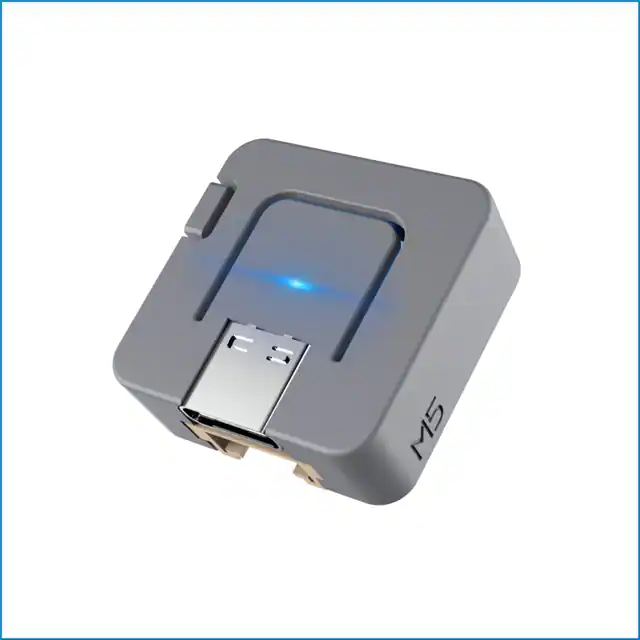
-
C008
M5Stack Technology Co., Ltd.
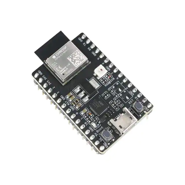
-
ESP32-C3-DEVKITC-02
Espressif Systems
-
ESP32-C6-DEVKITC-1-N8
Espressif Systems
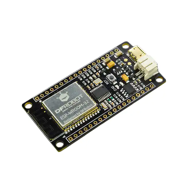
-
DFR0478
DFRobot
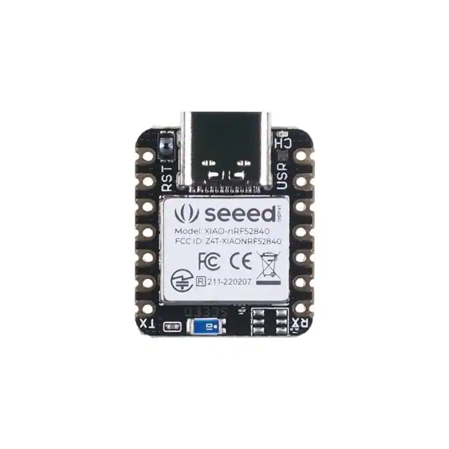
-
102010448
Seeed Technology Co., Ltd
-
ESP32-DEVKITC-32E
Espressif Systems
-
ESP32-DEVKITC-32UE
Espressif Systems
Tech Hub

A practical engineering guide to 3.3V and 5V logic compatibility, input thresholds, resistor dividers, translator ICs, MOSFET level shifting, I2C pull-ups, timing limits and power-sequencing risks.

The 74HC595 uses push-pull logic outputs, while the TPIC6B595 uses 50 V open-drain DMOS sinks for higher-power loads. This guide compares timing, current limits, 3.3 V interfacing, load wiring, thermal…

The 74HC595 converts serial data into eight stable parallel outputs. This guide covers pin functions, shift and storage timing, OE and MR behavior, drive-current limits, cascading, voltage compatibilit…

A technical comparison of level-sensitive latches and edge-triggered flip-flops, covering timing windows, setup and hold limits, master–slave operation, time borrowing, race-through, HDL inference and…

A D latch stores one bit while Enable controls when data can pass. This reference covers gate-level operation, truth tables, transparency, setup and hold timing, LE versus OE, common ICs and practical …

An SR latch stores one bit through cross-coupled feedback. This engineering reference covers NOR and NAND implementations, truth tables, forbidden-state recovery, gated operation, switch debouncing, fa…

Latch circuits retain one bit through feedback. This technical reference covers SR and D latches, truth tables, transparency, timing limits, latch-versus-flip-flop behavior, applications and common log…

An engineering guide to LED driver operation, constant-current and constant-voltage outputs, linear and switching topologies, dimming, IC selection, calculations, replacement compatibility, and fault c…

Operational amplifier guide covering op amp basics, feedback, ideal vs real op amps, common configurations, buffer circuits, offset, bias current, gain-bandwidth, slew rate, rail-to-rail limits and sel…

Jumper cables guide covering safe connection order, red and black clamp placement, final ground connection, cable gauge, length, clamp quality, copper vs CCA cables, jump starter comparison and battery…


