
 My Inquiry
 My Account


Renesas R5F10EGCAFB#V0
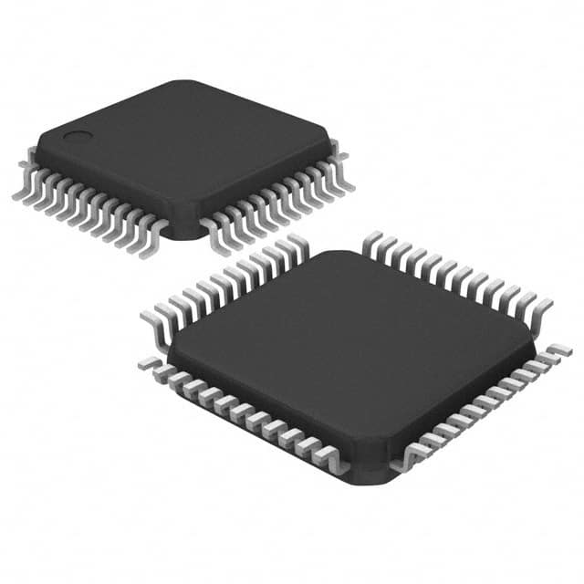
- Part No.:
- R5F10EGCAFB#V0
- Manufacturer:
- Renesas
- Category:
- Microcontrollers
- Package:
- 48-LQFP
- Datasheet:
-
 R5F10EGCAFB#V0.pdf
- Description:
- IC MCU 16BIT 32KB FLASH 48LFQFP
- Quantity:
- Payment:

- Shipping:

Inventory:1,247
Please send an inquiry. Send us your inquiry, and we will respond immediately.
Product details
Overview
R5F10EGCAFB#V0 from Renesas Electronics is a 48-pin LFQFP-packaged 16-bit RL78/G1A microcontroller with 32 KB flash, 4 KB data flash, 2 KB RAM, 12-bit 24-channel ADC, and ultra-low-power operation (66 µA/MHz active, 0.57 µA RTC+LVD). It integrates UART, I²C, SPI, RTC, PWM, and on-chip debug for battery-powered industrial sensor nodes and smart metering interfaces.
For engineers reviewing the R5F10EGCAFB#V0 datasheet, R5F10EGCAFB#V0 pinout, R5F10EGCAFB#V0 application, or R5F10EGCAFB#V0 equivalent, this page delivers verified specifications, package-confirmed pin functions, real-world use cases, and validated alternative options for design-in and supply continuity planning.
Technical Context
The R5F10EGCAFB#V0 implements the RL78 CPU core with Harvard architecture, 3-stage pipeline, and 86% of instructions executed in 1–2 cycles. It supports 32 MHz max operation via high-speed on-chip oscillator (±1% accuracy) or external crystal (X1/X2), with subsystem clock input (XT1/XT2) for RTC synchronization.
Its peripheral set includes dual serial array units (up to 6 I²C masters, 3 UARTs, 6 simplified SPI), 8-channel 16-bit timer array with PWM capability, DMA controller (2 channels), and safety features including flash CRC, RAM parity, and illegal memory access detection per IEC/UL 60730.
Key Specifications
| Parameter | Value and Actual Design Meaning |
|---|---|
| Core | 16-bit RL78 CPU with 41 DMIPS @ 32 MHz; CISC Harvard architecture enables deterministic real-time control. |
| Flash / Data Flash / RAM | 32 KB code flash, 4 KB background-operable data flash (1M erase cycles), 2 KB RAM with backup retention in all low-power modes. |
| Power Consumption | 66 µA/MHz active; 0.57 µA in Halt mode (RTC + LVD enabled); supports battery life extension in always-on sensing applications. |
| Analog Peripherals | 12-bit ADC with 24 input channels, 3.375 µs conversion time, internal 1.45 V reference, and on-chip temperature sensor. |
| Communication Interfaces | Up to 3 UARTs (7–9 bit), 6 I²C masters, 6 simplified SPI (CSI), LIN support, and I²C multi-master capability for distributed sensor networks. |
| Timers & Clock | 8-channel 16-bit timer array, RTC with full calendar/alarm/correction, 12-bit interval timer, and 15 kHz watchdog with window function. |
| Operating Range | −40 °C to +85 °C ambient; 1.6 V to 3.6 V single-supply operation enables direct connection to Li-ion or coin-cell sources. |
Pinout & Package
Package: 48-pin LFQFP (7 × 7 mm, 0.5 mm pitch), tray-packed (#V0).
| Pin/Terminal | Circuit Role | Design Meaning |
|---|---|---|
| P02/ANI17/TxD1/TI00 | Port 0 pin 2 / Analog input 17 / UART1 transmit / Timer input 0 | Multi-function I/O supporting simultaneous analog sensing and serial communication; configurable via PIOR register. |
| P03/ANI16/RxD1/TO00 | Port 0 pin 3 / Analog input 16 / UART1 receive / Timer output 0 | Enables hardware-triggered ADC sampling synchronized with UART frame timing or timer events. |
| P10/ANI18/SCK00/SCL00 | Port 1 pin 0 / Analog input 18 / SPI0 clock / I²C0 clock | Dual-role pin allows shared physical interface between SPI and I²C peripherals-reduces PCB routing complexity. |
| P11/ANI20/SI00/SDA00/RxD0/TOOLRxD | Port 1 pin 1 / Analog input 20 / SPI0 input / I²C0 data / UART0 receive / Debug RX | Combines debug interface, serial comms, and analog sensing on one pin-critical for space-constrained embedded designs. |
| P12/ANI21/SO00/TxD0/TOOLTxD | Port 1 pin 2 / Analog input 21 / SPI0 output / I²C0 data / UART0 transmit / Debug TX | Supports concurrent UART0 debug logging and SPI sensor readout without external multiplexing. |
| P20/ANI0/AVREFP | Port 2 pin 0 / Analog input 0 / ADC reference positive | Direct AVREFP connection enables precise ratiometric measurements using external voltage dividers or sensors. |
| P21/ANI1/AVREFM | Port 2 pin 1 / Analog input 1 / ADC reference negative | AVREFM tie to ground or external bias sets ADC full-scale range; supports differential measurement configurations. |
| P30/ANI27/SCK11/SCL11/INTP3/RTC1HZ | Port 3 pin 0 / Analog input 27 / SPI1 clock / I²C1 clock / Interrupt 3 / RTC 1 Hz output | RTC1HZ output provides accurate timebase for low-power wake-up scheduling without external components. |
| P31/ANI29/TI03/TO03/INTP4 | Port 3 pin 1 / Analog input 29 / Timer input 3 / Timer output 3 / Interrupt 4 | Hardware-coupled timer capture/compare enables precise pulse-width measurement or motor phase control. |
| P60/SCLA0 | Port 6 pin 0 / I²C0 clock (open-drain) | Open-drain SCLA0 requires external pull-up; supports standard/fast-mode I²C up to 400 kHz. |
| P61/SDAA0 | Port 6 pin 1 / I²C0 data (open-drain) | SDAA0 shares bus with SCLA0; enables multi-master arbitration and slave addressing in sensor hub topologies. |
| RESET | Active-low reset input | Accepts both power-on reset and external push-button assertion; LVD-interrupt capability prevents brown-out corruption. |
| REGC | Regulator capacitor terminal | Must connect 0.47–1 µF capacitor to VSS to stabilize internal voltage regulator-failure causes erratic low-power behavior. |
| VDD / VSS | Digital power supply / Ground | Single 1.6–3.6 V rail powers digital logic; decoupling near VDD/VSS pins required for EMI suppression at 32 MHz. |
| AVDD / AVSS | Analog power supply / Analog ground | Separate analog domain minimizes noise coupling into ADC; recommended to tie AVSS to VSS at single point. |
Key Features
| Feature | Design Value |
|---|---|
| Ultra-low-power operation | 0.57 µA Halt mode (RTC + LVD) enables >10-year battery life in wireless sensor endpoints with periodic wake-up. |
| On-chip debug interface | 1-wire TOOL0/TOOLRxD/TOOLTxD eliminates need for JTAG header-reduces board area and BOM cost. |
| Data flash with background operation | 4 KB data flash supports firmware parameter storage and field updates without halting application execution. |
| Hardware safety mechanisms | CRC calculation, RAM parity, SFR write protection, and illegal memory access detection meet IEC 60730 Class B requirements. |
| Flexible peripheral routing | Peripheral I/O redirection register (PIOR) allows dynamic remapping of UART/I²C/SPI functions to alternate pins-improves layout flexibility. |
| High-accuracy internal oscillator | 32 MHz on-chip oscillator ±1% over voltage/temperature eliminates external crystal for cost-sensitive timing-critical applications. |
Applications
| Smart Energy Metering | Industrial Sensor Node |
|---|---|
|
Use Scenario: Residential electricity meter with tamper detection, load profiling, and RF communication. IC Role / Device Role / Timing Role: Main controller managing ADC sampling of current/voltage transformers, RTC-based billing intervals, and UART-to-PLC modem interface. Use Value: 24-channel 12-bit ADC captures harmonic distortion; 0.57 µA Halt mode extends battery backup to 5+ years during power outage. |
Use Scenario: Wireless vibration/temperature node in predictive maintenance system deployed in factory machinery. IC Role / Device Role / Timing Role: Edge processor acquiring analog sensor data, performing FFT preprocessing, and triggering BLE transmission on threshold breach. Use Value: Snooze mode (0.6 mA ADC) enables continuous sampling while minimizing energy; PIOR allows reuse of same PCB for multiple sensor variants. |
| Home Appliance Control | Medical Wearable Monitor |
|
Use Scenario: Smart washing machine with water level, temperature, and motor current monitoring plus user interface. IC Role / Device Role / Timing Role: System MCU coordinating motor drivers, touch UI, and fault-safe thermal shutdown via LVD interrupt. Use Value: 32 KB flash accommodates bootloader + application + OTA update image; 20 mA I/O drive directly controls LED indicators and relays. |
Use Scenario: Portable ECG patch requiring long battery life, signal integrity, and regulatory compliance. IC Role / Device Role / Timing Role: Signal acquisition MCU handling analog front-end conditioning, 12-bit ADC oversampling, and secure data logging to data flash. Use Value: On-chip temperature sensor calibrates ADC offset drift; flash CRC and RAM parity satisfy IEC 62304 software safety classification. |
Equivalent & Alternatives
The following parts are listed as comparable options for similar microcontroller applications.
| Alternative Part | Technical Difference | Application Difference | Selection Advice |
|---|---|---|---|
| R5F10EGDABG#U0 | Same RL78/G1A core, 48 KB flash, 4 KB data flash, 3 KB RAM, 64-pin VFBGA package (4 × 4 mm). | Higher memory capacity and smaller footprint suit space-constrained designs needing firmware expansion headroom. | Select when >32 KB application code size is anticipated or PCB area is premium; requires re-layout due to BGA vs QFP. |
| R5F10EBCANA#00 | 32-pin HWQFN variant, 16 KB flash, 2 KB RAM, identical peripheral set but fewer I/O (26 total vs 42). | Lower pin count and reduced memory target cost-sensitive consumer devices with simpler I/O requirements. | Choose for compact remote controls or basic sensor transmitters where 26 GPIO and 16 KB flash suffice. |
Compared with R5F10EGCAFB#V0, R5F10EGDABG#U0 offers greater memory and density at the cost of soldering complexity, while R5F10EBCANA#00 trades I/O count and flash for lower unit cost and smaller footprint-enabling tiered product family scaling.
Availability
R5F10EGCAFB#V0 is available at Aetrix Electronics and suitable for industrial sensor nodes, smart metering interfaces, and home appliance control systems requiring stable component supply across multi-year production cycles.
Supply support for R5F10EGCAFB#V0 includes scheduled delivery planning, volume procurement assistance, BOM continuity management, traceable sourcing, and lifecycle availability coordination for OEM customers, industrial embedded developers, connected-device designers, and electronics production programs.
Manufacturer
Renesas Electronics is a global semiconductor leader specializing in microcontrollers, analog, and power solutions for automotive, industrial, and IoT markets.
The RL78/G1A product line targets ultra-low-power embedded applications demanding high integration, functional safety, and rapid time-to-market-optimized for battery-operated and energy-harvesting systems.
FAQ
What is the maximum operating frequency and power consumption of the R5F10EGCAFB#V0?
The R5F10EGCAFB#V0 operates at up to 32 MHz using its high-speed on-chip oscillator (±1% accuracy) and achieves 41 DMIPS performance. Its active power consumption is 66 µA per MHz, dropping to 0.57 µA in Halt mode with RTC and LVD enabled-making it ideal for battery-powered applications where runtime is critical. The R5F10EGCAFB#V0 maintains these values across its full 1.6–3.6 V supply range.
Does the R5F10EGCAFB#V0 support hardware debugging without external tools?
Yes, the R5F10EGCAFB#V0 includes a 1-wire on-chip debug interface accessible via TOOL0, TOOLRxD, and TOOLTxD pins. This eliminates the need for external JTAG/SWD debug probes during development and field programming. Engineers can perform full breakpoint debugging, memory inspection, and flash programming directly through the R5F10EGCAFB#V0's dedicated debug pins without adding connectors or circuitry.
How many analog input channels does the R5F10EGCAFB#V0 support, and what is the ADC resolution?
The R5F10EGCAFB#V0 integrates a 12-bit successive-approximation ADC with up to 24 input channels (ANI0–ANI29, excluding reserved pins). Conversion time is 3.375 µs, and it supports internal 1.45 V reference voltage, AVREFP/AVREFM inputs, and on-chip temperature sensing. This ADC configuration is confirmed for the 48-pin LFQFP package variant R5F10EGCAFB#V0 per Renesas datasheet R01DS0151EJ0230.
Can the R5F10EGCAFB#V0 operate from a single 1.8 V supply, and what low-power modes are available?
Yes, the R5F10EGCAFB#V0 supports operation from 1.6 V to 3.6 V, including stable functionality at 1.8 V. It offers four low-power modes: Stop (0.23 µA RAM-retained), Halt (0.57 µA with RTC+LVD), Snooze (0.6–0.7 mA with UART/ADC active), and Ultra-low-power Sleep (not specified in datasheet for this variant). These modes are fully supported in the R5F10EGCAFB#V0 and enable aggressive energy budgeting in portable and remote applications.
What safety certifications or built-in features does the R5F10EGCAFB#V0 include for industrial use?
The R5F10EGCAFB#V0 includes hardware-level safety features aligned with IEC/UL 60730 Class B requirements: flash memory CRC calculation, RAM parity error checking, SFR write protection, illegal memory access detection, clock stop/frequency monitoring, and ADC self-test. These are implemented in silicon-not software-and apply directly to the R5F10EGCAFB#V0 variant, enabling certified functional safety in industrial control and medical auxiliary systems.
R5F10EGCAFB#V0 Specifications
- Product attributes
- Attribute value
- Manufacturer:
- Renesas
- Package/Case:
- 48-LQFP
- Series:
- RL78/G1A
- Packaging:
- Tray
- Product Status:
- Active
- Programmable:
- Not Verified
- Core Processor:
- RL78
- Core Size:
- 16-Bit
- Speed:
- 32MHz
- Connectivity:
- CSI, I2C, LINbus, UART/USART
- Peripherals:
- DMA, LVD, POR, PWM, WDT
- Number of I/O:
- 32
- Program Memory Size:
- 32KB (32K x 8)
- Program Memory Type:
- FLASH
- EEPROM Size:
- -
- RAM Size:
- 2K x 8
- Voltage - Supply (Vcc/Vdd):
- 1.6V ~ 3.6V
- Data Converters:
- A/D 24x12b
- Oscillator Type:
- Internal
- Operating Temperature:
- -40°C ~ 85°C (TA)
- Grade:
- -
- Qualification:
- -
- Mounting Type:
- Surface Mount
- Supplier Device Package:
R5F10EGCAFB#V0 FAQ
1.How can I place an order for R5F10EGCAFB#V0 through Aetrix?
Please submit a Request for Quotation (RFQ) for R5F10EGCAFB#V0 on Aetrix. Our sales agent will provide a competitive quotation and guide you through the order confirmation once you accept the terms.
2.Are the price and stock information for R5F10EGCAFB#V0 reliable?
The price and inventory of R5F10EGCAFB#V0 are updated periodically and may fluctuate due to market conditions. Stock and pricing data are typically refreshed every 24 hours. Quotation validity for R5F10EGCAFB#V0 is usually 5 days.
3.What payment methods are accepted for R5F10EGCAFB#V0?
We accept Wire Transfer, PayPal, Credit Card, Western Union, MoneyGram, and Escrow for R5F10EGCAFB#V0 transactions.
Note: Certain payment methods may incur a processing fee.
4.How is shipping managed for R5F10EGCAFB#V0?
R5F10EGCAFB#V0 orders can be shipped via leading logistics carriers, including DHL, UPS, FedEx, TNT, or Registered Mail.
Once your R5F10EGCAFB#V0 order is processed, you will receive an email with the shipment details and tracking number.
Note: Tracking information may take up to 24 hours to appear. Express delivery typically takes 3–5 business days.
5.How can I obtain technical support or documentation for R5F10EGCAFB#V0?
For technical support, including R5F10EGCAFB#V0 datasheets, pinout diagrams, or application guidance, please contact our engineering support team. They can provide detailed documentation and assistance for your R5F10EGCAFB#V0 requirements.
6.How does Aetrix verify that R5F10EGCAFB#V0 is sourced from the original manufacturer or authorized distributors?
All R5F10EGCAFB#V0 products on Aetrix are procured from qualified distributors and authorized channels. Our dedicated quality assurance team conducts strict verification, including traceability checks and, if necessary, third-party testing. This ensures that R5F10EGCAFB#V0 meets industry standards.
7.What is the process for return or replacement of R5F10EGCAFB#V0?
All R5F10EGCAFB#V0 units undergo pre-shipment inspection (PSI). If there is an issue with R5F10EGCAFB#V0, returns or replacements are accepted under the following conditions:
1.Quantity discrepancies, incorrect items, or visible external defects (such as breakage or corrosion), acknowledged by Aetrix.
2.The issue is reported within 90 days of delivery.
3.The R5F10EGCAFB#V0 part is unused and in its original packaging.
Return procedure for R5F10EGCAFB#V0:
1.Submit a request within 90 days.
2.Obtain a Return Material Authorization (RMA) from Aetrix.
R5F10EGCAFB#V0 Tags

-
ATTINY4-TSHR
Microchip Technology
-
ATTINY10-TSHR
Microchip Technology
-
ATTINY10-TS8R
Microchip Technology

-
ATTINY202-SSNR
Microchip Technology
-
ATTINY202-SSFR
Microchip Technology
-
ATTINY402-SSNR
Microchip Technology

-
PIC16F15213T-I/MF
Microchip Technology
-
PIC16F15213-E/MF
Microchip Technology

-
PIC10F200T-I/OT
Microchip Technology
-
ATTINY412-SSNR
Microchip Technology
-
PIC10F202T-I/OT
Microchip Technology

-
ATTINY404-SSNR
Microchip Technology
Tech Hub

A practical engineering and sourcing framework covering lifecycle verification, lifetime-buy calculations, replacement qualification, supplier checks and counterfeit-risk controls.

TTL and CMOS logic families differ in thresholds, loading, output drive, power and timing. This engineering guide compares 74HC and 74HCT, calculates noise margins and checks 3.3 V/5 V compatibility.

A practical engineering guide to 3.3V and 5V logic compatibility, input thresholds, resistor dividers, translator ICs, MOSFET level shifting, I2C pull-ups, timing limits and power-sequencing risks.

The 74HC595 uses push-pull logic outputs, while the TPIC6B595 uses 50 V open-drain DMOS sinks for higher-power loads. This guide compares timing, current limits, 3.3 V interfacing, load wiring, thermal…

The 74HC595 converts serial data into eight stable parallel outputs. This guide covers pin functions, shift and storage timing, OE and MR behavior, drive-current limits, cascading, voltage compatibilit…

A technical comparison of level-sensitive latches and edge-triggered flip-flops, covering timing windows, setup and hold limits, master–slave operation, time borrowing, race-through, HDL inference and…

A D latch stores one bit while Enable controls when data can pass. This reference covers gate-level operation, truth tables, transparency, setup and hold timing, LE versus OE, common ICs and practical …

An SR latch stores one bit through cross-coupled feedback. This engineering reference covers NOR and NAND implementations, truth tables, forbidden-state recovery, gated operation, switch debouncing, fa…

Latch circuits retain one bit through feedback. This technical reference covers SR and D latches, truth tables, transparency, timing limits, latch-versus-flip-flop behavior, applications and common log…

An engineering guide to LED driver operation, constant-current and constant-voltage outputs, linear and switching topologies, dimming, IC selection, calculations, replacement compatibility, and fault c…


