
 My Inquiry
 My Account


Renesas R5F11AGJANB#20
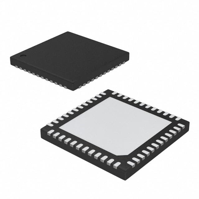
- Part No.:
- R5F11AGJANB#20
- Manufacturer:
- Renesas
- Category:
- Microcontrollers
- Package:
- 48-WFQFN Exposed Pad
- Datasheet:
-
 R5F11AGJANB#20.pdf
- Description:
- IC MCU 16BIT 256KB FLASH 48HWQFN
- Quantity:
- Payment:

- Shipping:

Inventory:380
Please send an inquiry. Send us your inquiry, and we will respond immediately.
Product details
Overview
R5F11AGJANB#20 from Renesas Electronics is a Bluetooth Low Energy 4.2 single-mode SoC MCU integrating a 16-bit RL78-S2 CPU core, on-chip 2.4 GHz RF transceiver, 256 KB flash, 20 KB RAM, and 8 KB data flash. It operates from 1.6 V to 3.6 V across –40°C to +85°C and targets ultra-low-power wearable sensors and BLE peripheral devices.
For engineers reviewing the R5F11AGJANB#20 datasheet, R5F11AGJANB#20 pinout, R5F11AGJANB#20 application, or R5F11AGJANB#20 equivalent, key selection criteria include integrated BLE v4.2 compliance, RF sleep current of 0.3 μA, 48-pin HWQFN package with RF-specific GPIOs (GPIO0–GPIO3), and support for AES-encrypted over-the-air updates in embedded BLE node designs.
Technical Context
The R5F11AGJANB#20 implements a Harvard-architecture RL78-S2 CPU with 3-stage pipeline, supporting instruction execution times from 0.03125 μs (@32 MHz) to 30.5 μs (@32.768 kHz). Its RF subsystem includes GFSK modulation, TDMA/TDD frequency hopping, and an integrated AES encryption circuit - all dedicated to slave-mode operation per Bluetooth v4.2 LE specifications.
It features dual-clock domains: a main system clock (up to 32 MHz via high-speed on-chip oscillator or external crystal) and a dedicated 32.768 kHz RF slow clock. The RF unit uses separate analog power rails (AVDD_RF/VSS_RF) and provides four GPIOs (GPIO0–GPIO3) for external PA/LNA control and clock output (CLKOUT_RF/EXSLK_RF).
Key Specifications
| Parameter | Value and Actual Design Meaning |
|---|---|
| CPU Core | 16-bit RL78-S2 CISC with 3-stage pipeline; enables deterministic real-time control at ultra-low power. |
| Flash / RAM / Data Flash | 256 KB main flash, 20 KB RAM, 8 KB background-operable data flash; supports secure boot swap and flash shield window. |
| RF Compliance | Bluetooth v4.2 Low Energy Single Mode only; certified for slave-device operation with adaptive frequency hopping. |
| Power Consumption | RF transmit: 4.3 mA (TYP); RF receive: 3.5 mA (TYP); RF POWER_DOWN: 0.3 μA (TYP); enables multi-year battery life in coin-cell applications. |
| Operating Voltage / Temp | 1.6 V to 3.6 V supply; –40°C to +85°C ambient; supports industrial-grade deployment without derating. |
| Package | 48-pin HWQFN (6 × 6 mm, 0.4 mm pitch); exposes die pad (GND1) and separates RF/analog ground (VSS_RF/AVSS_RF) for EMI-sensitive BLE layout. |
| Analog Peripherals | 8-channel 8/10-bit ADC (1.6–3.6 V range), internal 1.45 V reference, and temperature sensor; enables direct sensor interface without external signal conditioning. |
Pinout & Package
48-pin HWQFN (6 × 6 mm, 0.4 mm pitch) with exposed thermal pad (GND1). RF section uses dedicated power/ground pins (VDD_RF, AVDD_RF, VSS_RF, AVSS_RF) and crystal connections (XTAL1_RF/XTAL2_RF). Antenna interface is single-ended via ANT pin.
| Pin/Terminal | Circuit Role | Design Meaning |
|---|---|---|
| ANT | RF antenna interface | Single-ended 50 Ω output; requires matching network and PCB antenna or external balun for optimal BLE link budget. |
| GPIO0/TXSELH_RF GPIO1/TXSELL_RF | RF PA/LNA control outputs | Direct CMOS-level signals for high-side/low-side enable of external RF front-end components. |
| GPIO2/CLKOUT_RF GPIO3/EXSLK_RF | RF clock I/O | Provides 16/8/4 MHz RF clock output or accepts 32.768 kHz external slow clock for RF block timing synchronization. |
| XTAL1_RF / XTAL2_RF | RF crystal oscillator inputs | Dedicated 32 MHz crystal connection for RF baseband; isolated from main system clock domain to prevent interference. |
| DCLOUT / DCLIN | DC-DC converter interface | Supports integrated DC-DC regulator for improved RF efficiency; requires external inductor and capacitor per design guidelines. |
| REGC | Regulator capacitance terminal | Connects to VSS via 0.47–1 µF capacitor to stabilize internal voltage regulator for RF analog circuitry. |
Key Features
| Feature | Design Value |
|---|---|
| Integrated BLE v4.2 LE Transceiver | Eliminates need for external RF IC and associated RF layout complexity; reduces BOM count and PCB area by >30% in BLE peripherals. |
| AES Encryption Hardware | Accelerates over-the-air security operations in firmware updates and encrypted service communication without CPU overhead or software library dependencies. |
| Ultra-Low RF Sleep Current | 0.3 μA POWER_DOWN mode enables multi-year operation on CR2032 batteries in periodic-scan beacon or sensor-reporting applications. |
| Dual Power Domain Isolation | Separate VDD_RF/AVDD_RF and VSS_RF/AVSS_RF pins allow independent RF/analog grounding - critical for meeting FCC/ETSI radiated emission limits. |
| Background Data Flash Operation | Enables firmware self-update or parameter logging during active application runtime without interrupting BLE advertising or connection states. |
Applications
| Smart Wearable Sensor Node | BLE Proximity Tag |
|---|---|
Use Scenario: Compact wrist-worn health monitor collecting heart rate, temperature, and motion data. IC Role / Device Role / Timing Role: Primary SoC handling sensor acquisition, BLE advertising/connection, and secure OTA updates. Use Value: Integrated 8-channel ADC and BLE radio reduce component count; 0.3 μA RF sleep extends battery life beyond 12 months on a single coin cell. | Use Scenario: Asset tracking tag attached to equipment, broadcasting location and status via iBeacon/Eddystone. IC Role / Device Role / Timing Role: Standalone BLE broadcaster using RTC alarm and interval timer for scheduled low-duty-cycle transmissions. Use Value: 256 KB flash stores multiple beacon profiles and firmware; 4.3 mA TX current ensures reliable 30+ meter range in indoor environments. |
| Industrial Wireless Sensor | Medical Diagnostic Patch |
Use Scenario: Battery-powered temperature/humidity sensor deployed in factory HVAC ducts. IC Role / Device Role / Timing Role: Edge node performing local A/D conversion, data filtering, and BLE connection to gateway. Use Value: Operating voltage down to 1.6 V allows use of aging primary cells; –40°C to +85°C rating ensures reliability in uncontrolled environments. | Use Scenario: Disposable ECG patch transmitting raw waveform data to smartphone via BLE connection. IC Role / Device Role / Timing Role: Real-time signal processor with 10-bit ADC sampling at 1 kHz and low-latency BLE streaming. Use Value: On-chip 32.768 kHz oscillator drives precise RTC for time-stamped diagnostics; AES hardware secures patient data transmission. |
Equivalent & Alternatives
The following parts are listed as comparable options for similar BLE SoC applications.
| Alternative Part | Technical Difference | Application Difference | Selection Advice |
|---|---|---|---|
| nRF52833 DK | ARM Cortex-M4F core, 512 KB flash, 128 KB RAM, Bluetooth 5.1, higher RF output (+8 dBm) | Requires external crystal and more complex RF layout; lacks integrated DC-DC and dedicated RF GPIOs | Preferred when higher throughput, longer range, or advanced Bluetooth features (e.g., mesh) are required. |
| CC2642R1F | ARM Cortex-M4F, 352 KB flash, 80 KB RAM, Bluetooth 5.0, integrated RF balun, lower RX sensitivity (–97 dBm) | Higher power consumption in RX mode (5.8 mA vs. 3.5 mA); no on-chip AES accelerator | Chosen for TI ecosystem integration and production scalability where RF layout simplification outweighs power trade-offs. |
Compared with nRF52833 DK and CC2642R1F, the R5F11AGJANB#20 delivers superior ultra-low-power performance in BLE slave roles, simpler RF integration via dedicated GPIOs and DC-DC support, and hardware-accelerated security - making it optimal for cost-sensitive, long-life, sensor-edge applications.
Availability
R5F11AGJANB#20 is available at Aetrix Electronics and suitable for smart wearables, industrial wireless sensors, and medical diagnostic patches requiring stable component supply, extended lifecycle support, and consistent RF performance across production batches.
Supply support for R5F11AGJANB#20 includes scheduled delivery planning, volume procurement assistance, BOM continuity management, traceable sourcing, and lifecycle availability coordination for OEM customers, industrial embedded developers, connected-device designers, and electronics production programs.
Manufacturer
Renesas Electronics is a global semiconductor leader delivering microcontrollers, analog, power, and SoC solutions for automotive, industrial, and IoT markets.
The RL78/G1D product line integrates BLE 4.2 radio and RL78 CPU in a single chip to simplify development of ultra-low-power wireless sensor nodes and consumer BLE peripherals.
FAQ
What is the maximum operating frequency of the R5F11AGJANB#20 CPU core?
The R5F11AGJANB#20 features a 16-bit RL78-S2 CPU core with a maximum operating frequency of 32 MHz, achievable using the high-speed on-chip oscillator in HS mode at VDD ≥ 2.7 V. At lower voltages (1.6–2.4 V), the max frequency scales down to 4–16 MHz depending on operating mode, ensuring robust timing across wide voltage ranges.
Does the R5F11AGJANB#20 support Bluetooth 5.x features such as long-range or higher data rates?
No, the R5F11AGJANB#20 implements Bluetooth v4.2 Low Energy Single Mode only. It does not support Bluetooth 5.x features including coded PHY (long range), 2 Mbps PHY, or advertising extensions. Its RF subsystem is strictly compliant with v4.2 LE specifications and operates exclusively in slave role with adaptive frequency hopping.
How much user-accessible RAM is available on the R5F11AGJANB#20?
The R5F11AGJANB#20 provides 20 KB of on-chip RAM, fully accessible to firmware for variables, stack, heap, and BLE protocol stack buffers. When self-programming functionality is enabled, usable RAM reduces to approximately 19 KB due to reserved space for flash write operations.
Can the R5F11AGJANB#20 operate without an external crystal?
Yes, the R5F11AGJANB#20 can operate without external crystals using its internal oscillators: a high-speed on-chip oscillator (1–32 MHz) for the main system clock and a 32.768 kHz on-chip oscillator for the RF slow clock. External crystals (X1, XT1, XTAL1_RF) are optional and used only when higher frequency accuracy or stability is required.
What RF-related GPIOs are available on the R5F11AGJANB#20 and what are their functions?
The R5F11AGJANB#20 provides four dedicated RF GPIOs: GPIO0/TXSELH_RF and GPIO1/TXSELL_RF control external high-side/low-side PA/LNA enable lines; GPIO2/CLKOUT_RF outputs 16/8/4 MHz RF clocks; GPIO3/EXSLK_RF accepts 32.768 kHz external slow clock input for RF block synchronization - all electrically isolated from main MCU I/O.
R5F11AGJANB#20 Specifications
- Product attributes
- Attribute value
- Manufacturer:
- Renesas
- Package/Case:
- 48-WFQFN Exposed Pad
- Series:
- RL78/G1D
- Packaging:
- Tray
- Product Status:
- Active
- Programmable:
- Not Verified
- Core Processor:
- RL78
- Core Size:
- 16-Bit
- Speed:
- 32MHz
- Connectivity:
- CSI, I2C, UART/USART
- Peripherals:
- DMA, LVD, POR, PWM, WDT
- Number of I/O:
- 32
- Program Memory Size:
- 256KB (256K x 8)
- Program Memory Type:
- FLASH
- EEPROM Size:
- 8K x 8
- RAM Size:
- 20K x 8
- Voltage - Supply (Vcc/Vdd):
- 1.6V ~ 3.6V
- Data Converters:
- A/D 8x10b
- Oscillator Type:
- Internal
- Operating Temperature:
- -40°C ~ 85°C (TA)
- Grade:
- -
- Qualification:
- -
- Mounting Type:
- Surface Mount
- Supplier Device Package:
R5F11AGJANB#20 FAQ
1.How can I place an order for R5F11AGJANB#20 through Aetrix?
Please submit a Request for Quotation (RFQ) for R5F11AGJANB#20 on Aetrix. Our sales agent will provide a competitive quotation and guide you through the order confirmation once you accept the terms.
2.Are the price and stock information for R5F11AGJANB#20 reliable?
The price and inventory of R5F11AGJANB#20 are updated periodically and may fluctuate due to market conditions. Stock and pricing data are typically refreshed every 24 hours. Quotation validity for R5F11AGJANB#20 is usually 5 days.
3.What payment methods are accepted for R5F11AGJANB#20?
We accept Wire Transfer, PayPal, Credit Card, Western Union, MoneyGram, and Escrow for R5F11AGJANB#20 transactions.
Note: Certain payment methods may incur a processing fee.
4.How is shipping managed for R5F11AGJANB#20?
R5F11AGJANB#20 orders can be shipped via leading logistics carriers, including DHL, UPS, FedEx, TNT, or Registered Mail.
Once your R5F11AGJANB#20 order is processed, you will receive an email with the shipment details and tracking number.
Note: Tracking information may take up to 24 hours to appear. Express delivery typically takes 3–5 business days.
5.How can I obtain technical support or documentation for R5F11AGJANB#20?
For technical support, including R5F11AGJANB#20 datasheets, pinout diagrams, or application guidance, please contact our engineering support team. They can provide detailed documentation and assistance for your R5F11AGJANB#20 requirements.
6.How does Aetrix verify that R5F11AGJANB#20 is sourced from the original manufacturer or authorized distributors?
All R5F11AGJANB#20 products on Aetrix are procured from qualified distributors and authorized channels. Our dedicated quality assurance team conducts strict verification, including traceability checks and, if necessary, third-party testing. This ensures that R5F11AGJANB#20 meets industry standards.
7.What is the process for return or replacement of R5F11AGJANB#20?
All R5F11AGJANB#20 units undergo pre-shipment inspection (PSI). If there is an issue with R5F11AGJANB#20, returns or replacements are accepted under the following conditions:
1.Quantity discrepancies, incorrect items, or visible external defects (such as breakage or corrosion), acknowledged by Aetrix.
2.The issue is reported within 90 days of delivery.
3.The R5F11AGJANB#20 part is unused and in its original packaging.
Return procedure for R5F11AGJANB#20:
1.Submit a request within 90 days.
2.Obtain a Return Material Authorization (RMA) from Aetrix.
R5F11AGJANB#20 Tags

-
ATTINY4-TSHR
Microchip Technology
-
ATTINY10-TSHR
Microchip Technology
-
ATTINY10-TS8R
Microchip Technology

-
ATTINY202-SSNR
Microchip Technology
-
ATTINY202-SSFR
Microchip Technology
-
ATTINY402-SSNR
Microchip Technology

-
PIC16F15213T-I/MF
Microchip Technology
-
PIC16F15213-E/MF
Microchip Technology

-
PIC10F200T-I/OT
Microchip Technology
-
ATTINY412-SSNR
Microchip Technology
-
PIC10F202T-I/OT
Microchip Technology

-
ATTINY404-SSNR
Microchip Technology
Tech Hub

TTL and CMOS logic families differ in thresholds, loading, output drive, power and timing. This engineering guide compares 74HC and 74HCT, calculates noise margins and checks 3.3 V/5 V compatibility.

A practical engineering guide to 3.3V and 5V logic compatibility, input thresholds, resistor dividers, translator ICs, MOSFET level shifting, I2C pull-ups, timing limits and power-sequencing risks.

The 74HC595 uses push-pull logic outputs, while the TPIC6B595 uses 50 V open-drain DMOS sinks for higher-power loads. This guide compares timing, current limits, 3.3 V interfacing, load wiring, thermal…

The 74HC595 converts serial data into eight stable parallel outputs. This guide covers pin functions, shift and storage timing, OE and MR behavior, drive-current limits, cascading, voltage compatibilit…

A technical comparison of level-sensitive latches and edge-triggered flip-flops, covering timing windows, setup and hold limits, master–slave operation, time borrowing, race-through, HDL inference and…

A D latch stores one bit while Enable controls when data can pass. This reference covers gate-level operation, truth tables, transparency, setup and hold timing, LE versus OE, common ICs and practical …

An SR latch stores one bit through cross-coupled feedback. This engineering reference covers NOR and NAND implementations, truth tables, forbidden-state recovery, gated operation, switch debouncing, fa…

Latch circuits retain one bit through feedback. This technical reference covers SR and D latches, truth tables, transparency, timing limits, latch-versus-flip-flop behavior, applications and common log…

An engineering guide to LED driver operation, constant-current and constant-voltage outputs, linear and switching topologies, dimming, IC selection, calculations, replacement compatibility, and fault c…

Operational amplifier guide covering op amp basics, feedback, ideal vs real op amps, common configurations, buffer circuits, offset, bias current, gain-bandwidth, slew rate, rail-to-rail limits and sel…


