
 My Inquiry
 My Account


Renesas R5F56514ADFP#30
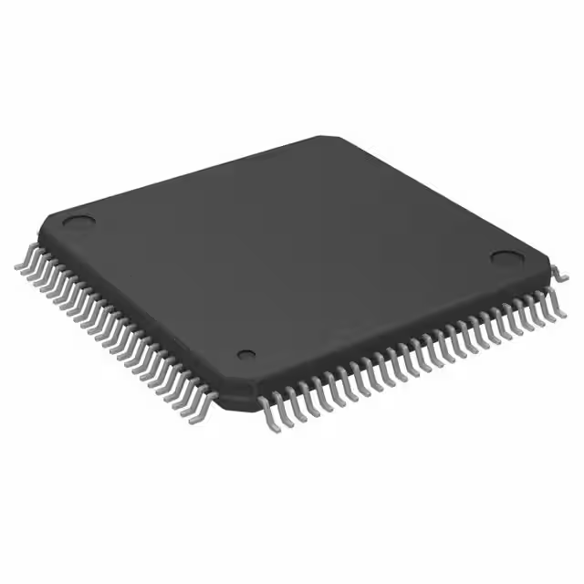
- Part No.:
- R5F56514ADFP#30
- Manufacturer:
- Renesas
- Category:
- Microcontrollers
- Package:
- 100-LQFP
- Datasheet:
-
 R5F56514ADFP#30.pdf
- Description:
- IC MCU 32BIT 512KB FLSH 100LFQFP
- Quantity:
- Payment:

- Shipping:

Inventory:552
Please send an inquiry. Send us your inquiry, and we will respond immediately.
Product details
Overview
Renesas R5F56514ADFP#30 is a 32-bit RX651 microcontroller based on the RXv2 CPU core. It operates at up to 120 MHz and integrates a single-precision floating-point unit, 512 KB of code flash, 256 KB of SRAM, USB full-speed host and device support, two CAN channels, extensive serial connectivity, timers, and mixed-signal peripherals.
Engineers comparing the R5F56514ADFP#30 datasheet, pinout, applications, or equivalents should note the exact device configuration: 100-pin LFQFP packaging, 2.7 V to 3.6 V operation, 79 I/O ports, 22-channel 12-bit ADC, one 12-bit DAC channel, no data flash, no SD host interface, no Ethernet controller, and no AES or TRNG engine.
Technical Context
R5F56514ADFP#30 combines a 120 MHz RXv2 core with 256 KB of zero-wait-state SRAM and a single-precision FPU, allowing control algorithms, digital filtering, communication protocol processing, and HMI coordination to run without an external application processor. Its 512 KB code-flash capacity places it in the lower-memory RX651 configuration, so firmware size, bootloader allocation, diagnostic code, and field-update space must be planned carefully.
This version does not include data flash or the dual-bank code-flash function available on larger-memory RX651 variants. Products requiring frequently updated calibration values, event logs, or EEPROM-style storage should therefore provide an external nonvolatile memory or another storage method with suitable endurance. Field-update firmware must also account for single-bank memory operation rather than assuming automatic start-up-bank exchange.
The 100-pin package exposes USB full-speed host/device capability, two CAN channels, QSPI, an 8- or 16-bit external memory bus, and numerous SCI-based serial modes. Many peripheral signals share the same physical pins, so UART, SPI, I2C, CAN, timer, external-bus, and analog assignments must be resolved together during board design. R5F56514ADFP#30 does not provide Ethernet, SDHI, a graphics LCD controller, or hardware AES/TRNG functions.
Key Specifications
| Parameter | Value and Actual Design Meaning |
|---|---|
| MCU Family | Renesas RX651 within the RX600 series, intended for general embedded control, connectivity, and HMI applications. |
| CPU Core | 32-bit RXv2 CISC core with a five-stage pipeline, fast interrupt handling, DSP instructions, and a 4 GB linear address space. |
| Maximum Operating Frequency | 120 MHz, providing up to 240 DMIPS under the RXv2 performance conditions. |
| Floating-Point Unit | Single-precision IEEE-754 FPU for control calculations, filtering, measurements, and other arithmetic-intensive firmware. |
| Code Flash | 512 KB of internal program flash. Firmware, bootloader, diagnostic, and update-space requirements must fit within this capacity. |
| Data Flash | Not included in R5F56514ADFP#30. Persistent configuration or logging may require external nonvolatile storage. |
| SRAM | 256 KB of internal SRAM for application data, communication buffers, control variables, and runtime stacks. |
| Dual-Bank Flash | Not available on this 512 KB version. Firmware-update procedures must be designed for single-bank code-flash operation. |
| Supply Voltage | Single 2.7 V to 3.6 V supply range for the main MCU operating domains. |
| Operating Temperature | -40°C to +85°C ambient operating range for the D-temperature version. |
| I/O Ports | 79 I/O ports with extensive pin multiplexing; the number of simultaneously usable peripheral signals depends on the selected pin assignments. |
| External Interrupts | 16 external interrupt inputs for event detection, wake-up sources, and real-time control signals. |
| DMA Functions | Eight-channel DMAC together with DTC support, reducing CPU load during peripheral and memory transfers. |
| USB | One USB 2.0 full-speed controller supporting host and device operation, with dedicated USB power and differential data pins. |
| CAN | Two CAN channels supporting classical CAN communication up to 1 Mbps; CAN FD is not included. |
| Serial Communication | Eleven SCI/UART channels with multiple operating modes, together with up to 14 SPI-capable and 13 I2C-capable interface functions. Pin multiplexing determines the usable combination. |
| QSPI | One quad-SPI interface for connection to compatible external serial memories and peripherals. |
| External Memory Bus | 8-bit or 16-bit external bus support for parallel memory and peripheral expansion. A dedicated DRAM interface is not included. |
| Timer Resources | Three 32-bit timer channels, 18 16-bit timer channels, four 8-bit timer channels, RTC, watchdog timer, and up to 38 PWM-capable output pins. |
| Analog-to-Digital Converter | Twenty-two 12-bit ADC channels for sensor acquisition, control feedback, and system monitoring. |
| Digital-to-Analog Converter | One 12-bit DAC channel for analog control, reference generation, or waveform output. |
| Temperature Sensor | One internal temperature-sensor channel for monitoring MCU die-temperature changes. |
| Clock Resources | Main and sub-clock inputs, internal oscillators, PLL-based clock generation, and 32.768 kHz sub-clock support for RTC operation. |
| Reset and Monitoring | Power-on reset, low-voltage detection, watchdog timer, independent watchdog timer, and clock-failure monitoring support. |
| Security | Includes a unique device ID. R5F56514ADFP#30 does not include the AES or TRNG hardware available in selected RX651 variants. |
| Debug Interface | JTAG and FINE single-wire serial debugging support for programming, debugging, and production access. |
| Package | 100-pin LFQFP, 14 mm × 14 mm × 1.7 mm body, 0.5 mm lead pitch, package code PLQP0100KB-B. |
| Moisture Sensitivity | MSL 3, requiring controlled floor-life, storage, and reflow handling after the moisture-barrier packaging is opened. |
| Carrier and Compliance | R5F56514ADFP#30 is supplied in bulk tray packaging and is lead-free. |
Pinout & Package
R5F56514ADFP#30 uses a 100-pin LFQFP package with a 14 mm × 14 mm body, 1.7 mm maximum profile, and 0.5 mm lead pitch. The package combines dedicated power, clock, reset, USB, analog-reference, and debug pins with multiplexed I/O pins configured through the multi-function pin controller.
| Pin / Pin Group | Primary Function | Connection Guidance |
|---|---|---|
| Pins 14 and 60 - VCC | Main digital power supply | Connect to the 2.7 V to 3.6 V supply with local ceramic decoupling placed close to each power and ground pair. |
| Pins 12 and 62 - VSS | Digital ground | Connect to the system ground plane using short, low-impedance paths. |
| Pins 1 and 3 - AVCC1 / AVSS1 | Analog power and ground for the secondary analog domain | Use a clean supply and ground connection appropriate for the required analog measurement performance. |
| Pins 97 and 99 - AVCC0 / AVSS0 | Primary ADC and DAC power domain | Route with careful decoupling and separation from high-current or fast-switching return paths. |
| Pins 96 and 94 - VREFH0 / VREFL0 | ADC reference high and low | Connect to stable reference potentials because reference noise directly affects conversion accuracy. |
| Pin 5 - VCL | Internal voltage-regulator stabilization terminal | Connect the required external stabilization capacitor close to the pin with a short ground return. |
| Pin 6 - VBATT | Backup supply input | Supports RTC retention from a backup source when the main supply is unavailable. |
| Pins 11 and 13 - XTAL / EXTAL | Main oscillator connection | Connect the main resonator or external clock source using a short, symmetric, low-noise layout. |
| Pins 8 and 9 - XCIN / XCOUT | Sub-clock oscillator connection | Used with a 32.768 kHz resonator when accurate RTC or low-power timekeeping is required. |
| Pin 10 - RES# | Active-low external reset | Connect to the system reset network and maintain the required power-up and reset-release timing. |
| Pins 35 to 38 - VCC_USB, USB0_DM, USB0_DP, VSS_USB | USB power and differential interface | Route USB0_DM and USB0_DP as a controlled differential pair and decouple the USB supply close to the device. |
| Pins 2, 7, 16, and 19 to 22 | EMLE, MD/FINED, TRST#, TMS, TDI, TCK, and TDO debug or mode functions | Set the mode and emulator connections according to the selected JTAG, FINE, boot, or normal operating configuration. |
| Multiplexed Port Pins | GPIO, UART, SPI, I2C, CAN, QSPI, timers, external bus, interrupts, ADC, and DAC | Resolve all peripheral assignments before PCB layout because several desired functions may compete for the same physical pins. |
Key Features
- 120 MHz 32-bit RXv2 CPU core
- Single-precision IEEE-754 floating-point unit
- 512 KB internal code flash
- 256 KB internal SRAM
- Single 2.7 V to 3.6 V supply operation
- 79 multiplexed I/O ports
- USB 2.0 full-speed host and device capability
- Two classical CAN channels
- Eleven SCI/UART channels
- QSPI and extensive SPI- and I2C-capable serial functions
- Eight-channel DMAC with DTC support
- Twenty-two 12-bit ADC channels and one 12-bit DAC channel
- Extensive timer, PWM, RTC, watchdog, and event-control resources
- JTAG and FINE single-wire debugging
- 100-pin 14 mm × 14 mm LFQFP package
- -40°C to +85°C operating temperature range
- MSL 3 and lead-free construction
Applications
| Industrial HMI and Operator Panels | USB and CAN Communication Gateways |
|---|---|
|
Use Scenario: Control panels, user interfaces, instruments, and embedded terminals using external or serially connected display hardware. IC Role: R5F56514ADFP#30 executes interface logic, menu processing, system control, communication protocols, and local input monitoring. Use Value: The 120 MHz RXv2 core, FPU, 256 KB SRAM, timers, serial interfaces, and 79 I/O ports support responsive HMI control without requiring an integrated graphics controller. |
Use Scenario: Equipment requiring communication between USB, dual CAN networks, UART, SPI, or I2C-connected subsystems. IC Role: R5F56514ADFP#30 manages protocol processing, message buffering, diagnostics, and data transfer between connected interfaces. Use Value: USB host/device capability, two CAN channels, DMA resources, and multiple serial modes reduce the need for separate communication controllers. |
| Motor and Actuator Control | Mixed-Signal Monitoring and Data Acquisition |
|
Use Scenario: Motor drives, actuator controllers, power-conversion controls, and multi-channel PWM systems. IC Role: R5F56514ADFP#30 generates timing and PWM signals, samples control feedback, handles fault events, and executes real-time control calculations. Use Value: The FPU, fast interrupt response, timer resources, 38 PWM-capable outputs, ADC channels, and DMA functions support deterministic control implementation. |
Use Scenario: Industrial measurement, sensor aggregation, process monitoring, and embedded instrumentation. IC Role: R5F56514ADFP#30 acquires analog signals, performs filtering and scaling, stores working data in SRAM, and transfers results through USB, CAN, or serial interfaces. Use Value: Twenty-two 12-bit ADC channels, one 12-bit DAC channel, an internal temperature sensor, and an FPU provide a flexible mixed-signal control platform. |
Equivalent & Alternatives
R5F56514ADFP#30 alternatives are available within the RX651 family when a different tray option, SD host interface, or hardware cryptographic capability is required. Devices sharing the 100-pin LFQFP package, 512 KB code flash, 256 KB SRAM, 120 MHz RXv2 core, and -40°C to +85°C temperature range provide the closest migration path.
| Alternative Part | Technical Difference | Application Difference | Selection Advice |
|---|---|---|---|
| R5F56514ADFP#10 | Uses the same RX651 base device, 512 KB code flash, 256 KB SRAM, 120 MHz core, interface set, and 100-pin LFQFP format. The #10 version uses full-carton tray ordering instead of the #30 bulk-tray option. | Electrical functionality remains aligned with R5F56514ADFP#30, while procurement quantities, tray configuration, and eligible package-source variation differ. | This is the closest supply alternative. Confirm the exact package code, body thickness, tray quantity, marking, and manufacturing documentation before production approval. |
| R5F56514BDFP#30 | Retains the 512 KB flash, 256 KB SRAM, 120 MHz RXv2 core, 100-pin LFQFP package, USB, CAN, analog, and serial functions while adding one SD host interface. Security remains limited to the unique ID without AES or TRNG. | Suited to systems that require direct SD memory or SDIO connectivity while retaining the same core memory capacity and package class. | A close same-package functional upgrade. Revalidate pin multiplexing, peripheral initialization, option settings, firmware configuration, and PCB use of the SDHI-related pins. |
| R5F56514EDFP#30 | Matches the 512 KB flash, 256 KB SRAM, 120 MHz core, 100-pin LFQFP package, and main peripheral set while adding hardware AES and TRNG functions. It does not add SDHI. | Better suited to equipment requiring hardware-assisted encryption, random-number generation, authentication, or protected communications without an SD interface. | Consider as a security-enhanced migration option. Confirm firmware support for the cryptographic module and repeat pin, clock, boot, programming, and validation testing. |
| R5F56514FDFP#30 | Maintains the same core, memory capacity, supply range, temperature range, and 100-pin LFQFP package while adding both AES/TRNG security functions and one SD host interface. | Supports designs requiring local SD storage together with hardware-assisted cryptographic functions. | The broadest functional upgrade among the 512 KB DFP variants. Review multiplexed SDHI pins, security firmware, device configuration, qualification records, and production-programming settings before substitution. |
R5F56514ADFP#10 is the closest option when only the purchasing and tray configuration can change. R5F56514BDFP#30 adds SDHI, R5F56514EDFP#30 adds AES and TRNG, and R5F56514FDFP#30 adds both capabilities. Firmware and pin-multiplexing validation remain necessary even when the package and principal memory configuration match.
Quality
R5F56514ADFP#30 is an active, lead-free Renesas MCU with MSL 3 classification. Incoming inspection should verify Renesas traceability, ordering suffix, lot and date codes, original tray and moisture-barrier packaging, humidity-indicator condition, package marking, lead coplanarity, and evidence of oxidation or handling damage. Electrical or programmed sampling can confirm device identification, power-up behavior, flash programming, debug access, supply current, and selected I/O functions without assuming that visual marking alone proves device authenticity.
Availability
R5F56514ADFP#30 is available at Aetrix Electronics for prototype, maintenance, and production requirements, subject to current inventory, lead time, date-code acceptance, tray quantity, and traceability requirements. Renesas lists R5F56514ADFP#30 as active, while the RX651 family is covered by its product-longevity program through December 2041. Production buyers should confirm the #30 bulk-tray suffix and 100-pin PLQP0100KB-B package before purchase.
Manufacturer
R5F56514ADFP#30 is manufactured by Renesas Electronics as part of the RX651 group within the RX 32-bit microcontroller portfolio. Renesas supplies microcontrollers, analog and power devices, connectivity products, embedded processors, and development tools for industrial, automotive, infrastructure, consumer, and IoT applications.
FAQ
What type of microcontroller is R5F56514ADFP#30?
R5F56514ADFP#30 is a Renesas RX651 32-bit microcontroller built around the 120 MHz RXv2 CPU core. It integrates a single-precision FPU, 512 KB of code flash, 256 KB of SRAM, USB host and device support, two CAN channels, serial interfaces, timers, and mixed-signal peripherals in a 100-pin LFQFP package.
How much memory does R5F56514ADFP#30 include?
R5F56514ADFP#30 contains 512 KB of internal code flash and 256 KB of SRAM. It does not contain data flash and does not support the dual-bank flash function used by larger RX651 variants. Firmware size, bootloader allocation, update procedures, and persistent-data storage must therefore be planned around this specific memory configuration.
What package and pinout are used by R5F56514ADFP#30?
R5F56514ADFP#30 uses a 100-pin LFQFP package measuring 14 mm × 14 mm × 1.7 mm with 0.5 mm lead pitch. It includes dedicated power, ground, oscillator, reset, USB, analog-reference, and debug pins, while most communication, timer, external-bus, interrupt, ADC, and DAC signals share multiplexed port pins.
Which communication interfaces are available on R5F56514ADFP#30?
R5F56514ADFP#30 provides one USB 2.0 full-speed host/device controller, two classical CAN channels, 11 SCI/UART channels, one QSPI interface, and numerous SPI- and I2C-capable serial functions. It does not include Ethernet, CAN FD, or SDHI. Actual interface combinations depend on the selected multi-function pin assignments.
Does R5F56514ADFP#30 include data flash or hardware encryption?
R5F56514ADFP#30 does not include data flash, an AES engine, or a hardware true-random-number generator. It provides a unique device ID for identification purposes. Applications requiring EEPROM-style storage or hardware-assisted cryptography should add suitable external devices or consider an RX651 variant with the required integrated functions.
What analog and timer resources does R5F56514ADFP#30 provide?
R5F56514ADFP#30 includes 22 channels of 12-bit analog-to-digital conversion, one 12-bit DAC channel, an internal temperature sensor, three 32-bit timer channels, 18 16-bit timer channels, four 8-bit timer channels, and up to 38 PWM-capable outputs. These resources support measurement, motor control, waveform generation, and real-time automation.
How is R5F56514ADFP#30 programmed and debugged?
R5F56514ADFP#30 supports on-board flash programming and debugging through JTAG and the Renesas FINE single-wire serial interface. The MD/FINED, EMLE, reset, and JTAG-related pins must be configured correctly for the selected programming method. Production programming should use the correct RX651 device definition, flash range, option settings, and security configuration.
What alternatives can be considered for R5F56514ADFP#30?
R5F56514ADFP#10 is the closest alternative to R5F56514ADFP#30 when a different tray configuration is acceptable. R5F56514BDFP#30 adds SDHI, R5F56514EDFP#30 adds AES and TRNG, and R5F56514FDFP#30 adds both functions. Pin multiplexing, firmware, package records, and production-programming settings must be revalidated before substitution.
R5F56514ADFP#30 Specifications
- Product attributes
- Attribute value
- Manufacturer:
- Renesas
- Package/Case:
- 100-LQFP
- Series:
- RX651
- Packaging:
- Tray
- Product Status:
- Active
- Programmable:
- Not Verified
- Core Processor:
- RXv2
- Core Size:
- 32-Bit Single-Core
- Speed:
- 120MHz
- Connectivity:
- CANbus, EBI/EMI, Ethernet, I2C, LINbus, MMC/SD, QSPI, SCI, SPI, UART/USART, USB
- Peripherals:
- DMA, LVD, POR, PWM, WDT
- Number of I/O:
- 78
- Program Memory Size:
- 512KB (512K x 8)
- Program Memory Type:
- FLASH
- EEPROM Size:
- -
- RAM Size:
- 256K x 8
- Voltage - Supply (Vcc/Vdd):
- 2.7V ~ 3.6V
- Data Converters:
- A/D 22x12b; D/A 1x12b
- Oscillator Type:
- Internal
- Operating Temperature:
- -40°C ~ 85°C (TA)
- Grade:
- -
- Qualification:
- -
- Mounting Type:
- Surface Mount
- Supplier Device Package:
R5F56514ADFP#30 FAQ
1.How can I place an order for R5F56514ADFP#30 through Aetrix?
Please submit a Request for Quotation (RFQ) for R5F56514ADFP#30 on Aetrix. Our sales agent will provide a competitive quotation and guide you through the order confirmation once you accept the terms.
2.Are the price and stock information for R5F56514ADFP#30 reliable?
The price and inventory of R5F56514ADFP#30 are updated periodically and may fluctuate due to market conditions. Stock and pricing data are typically refreshed every 24 hours. Quotation validity for R5F56514ADFP#30 is usually 5 days.
3.What payment methods are accepted for R5F56514ADFP#30?
We accept Wire Transfer, PayPal, Credit Card, Western Union, MoneyGram, and Escrow for R5F56514ADFP#30 transactions.
Note: Certain payment methods may incur a processing fee.
4.How is shipping managed for R5F56514ADFP#30?
R5F56514ADFP#30 orders can be shipped via leading logistics carriers, including DHL, UPS, FedEx, TNT, or Registered Mail.
Once your R5F56514ADFP#30 order is processed, you will receive an email with the shipment details and tracking number.
Note: Tracking information may take up to 24 hours to appear. Express delivery typically takes 3–5 business days.
5.How can I obtain technical support or documentation for R5F56514ADFP#30?
For technical support, including R5F56514ADFP#30 datasheets, pinout diagrams, or application guidance, please contact our engineering support team. They can provide detailed documentation and assistance for your R5F56514ADFP#30 requirements.
6.How does Aetrix verify that R5F56514ADFP#30 is sourced from the original manufacturer or authorized distributors?
All R5F56514ADFP#30 products on Aetrix are procured from qualified distributors and authorized channels. Our dedicated quality assurance team conducts strict verification, including traceability checks and, if necessary, third-party testing. This ensures that R5F56514ADFP#30 meets industry standards.
7.What is the process for return or replacement of R5F56514ADFP#30?
All R5F56514ADFP#30 units undergo pre-shipment inspection (PSI). If there is an issue with R5F56514ADFP#30, returns or replacements are accepted under the following conditions:
1.Quantity discrepancies, incorrect items, or visible external defects (such as breakage or corrosion), acknowledged by Aetrix.
2.The issue is reported within 90 days of delivery.
3.The R5F56514ADFP#30 part is unused and in its original packaging.
Return procedure for R5F56514ADFP#30:
1.Submit a request within 90 days.
2.Obtain a Return Material Authorization (RMA) from Aetrix.
R5F56514ADFP#30 Tags

-
ATTINY4-TSHR
Microchip Technology
-
ATTINY10-TSHR
Microchip Technology
-
ATTINY10-TS8R
Microchip Technology

-
ATTINY202-SSNR
Microchip Technology
-
ATTINY202-SSFR
Microchip Technology
-
ATTINY402-SSNR
Microchip Technology

-
PIC16F15213T-I/MF
Microchip Technology
-
PIC16F15213-E/MF
Microchip Technology

-
PIC10F200T-I/OT
Microchip Technology
-
ATTINY412-SSNR
Microchip Technology
-
PIC10F202T-I/OT
Microchip Technology

-
ATTINY404-SSNR
Microchip Technology
Tech Hub

TTL and CMOS logic families differ in thresholds, loading, output drive, power and timing. This engineering guide compares 74HC and 74HCT, calculates noise margins and checks 3.3 V/5 V compatibility.

A practical engineering guide to 3.3V and 5V logic compatibility, input thresholds, resistor dividers, translator ICs, MOSFET level shifting, I2C pull-ups, timing limits and power-sequencing risks.

The 74HC595 uses push-pull logic outputs, while the TPIC6B595 uses 50 V open-drain DMOS sinks for higher-power loads. This guide compares timing, current limits, 3.3 V interfacing, load wiring, thermal…

The 74HC595 converts serial data into eight stable parallel outputs. This guide covers pin functions, shift and storage timing, OE and MR behavior, drive-current limits, cascading, voltage compatibilit…

A technical comparison of level-sensitive latches and edge-triggered flip-flops, covering timing windows, setup and hold limits, master–slave operation, time borrowing, race-through, HDL inference and…

A D latch stores one bit while Enable controls when data can pass. This reference covers gate-level operation, truth tables, transparency, setup and hold timing, LE versus OE, common ICs and practical …

An SR latch stores one bit through cross-coupled feedback. This engineering reference covers NOR and NAND implementations, truth tables, forbidden-state recovery, gated operation, switch debouncing, fa…

Latch circuits retain one bit through feedback. This technical reference covers SR and D latches, truth tables, transparency, timing limits, latch-versus-flip-flop behavior, applications and common log…

An engineering guide to LED driver operation, constant-current and constant-voltage outputs, linear and switching topologies, dimming, IC selection, calculations, replacement compatibility, and fault c…

Operational amplifier guide covering op amp basics, feedback, ideal vs real op amps, common configurations, buffer circuits, offset, bias current, gain-bandwidth, slew rate, rail-to-rail limits and sel…


