
 My Inquiry
 My Account


Renesas R5F56514EDLK#20
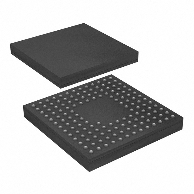
- Part No.:
- R5F56514EDLK#20
- Manufacturer:
- Renesas
- Category:
- Microcontrollers
- Package:
- 145-TFLGA
- Datasheet:
-
 R5F56514EDLK#20.pdf
- Description:
- IC MCU 32BIT 512KB FLSH 145TFLGA
- Quantity:
- Payment:

- Shipping:

Inventory:416
Please send an inquiry. Send us your inquiry, and we will respond immediately.
Product details
Overview
R5F56514EDLK#20 from Renesas Electronics is an RX65N Envision Kit - a hardware evaluation platform for the RX65N 32-bit microcontroller family, featuring a 120 MHz RXv2 CPU core, integrated 2 MB flash, 384 KB SRAM, and support for secure boot, capacitive touch, and USB host/device interfaces. It includes on-board debugging via JTAG/SWD, a 4.3-inch resistive touchscreen, and preloaded firmware for rapid validation of industrial HMI, secure firmware update, and dual-bank OTA workflows.
For engineers reviewing the R5F56514EDLK#20 datasheet, R5F56514EDLK#20 pinout, R5F56514EDLK#20 application, or R5F56514EDLK#20 equivalent, this page provides verified technical context, firmware update flow details, supported demo configurations (standard/benchmark), secure boot architecture, and board-level interface mapping - all essential for HMI prototyping, secure firmware development, and dual-bank field update validation.
Technical Context
The R5F56514EDLK#20 implements a dual-bank firmware update mechanism using the RX65N's built-in flash memory partitioning, enabling atomic bank swap and software reset without external intervention. Boot loader operation is triggered by SW2 long-press (≥3 s) and supports automatic *.rsu file loading from USB mass storage.
Firmware delivery relies on Renesas-provided convert.exe to transform *.mot files (generated from IAR/E2 studio projects) into *.rsu update packages compatible with the onboard bootloader. Demo projects include rx65n_secure_boot (bootloader), standard (HMI + touch control), and benchmark (performance profiling) - each compiled for the exact R5F56514EDLK#20 target configuration.
Key Specifications
| Parameter | Value and Actual Design Meaning |
|---|---|
| CPU Core | RXv2 32-bit, 120 MHz - enables real-time HMI rendering and cryptographic operations in secure boot flow. |
| Flash Memory | 2 MB on-chip flash, partitioned into primary/secondary banks - supports atomic firmware updates without data loss. |
| SRAM | 384 KB on-chip SRAM - sufficient for concurrent touch driver, GUI stack, and TLS handshake buffers. |
| Display Interface | 4.3-inch resistive touchscreen with parallel RGB interface - directly driven by RX65N's LCD controller, no external driver IC required. |
| USB Support | USB 2.0 full-speed host/device - used for firmware update via USB memory stick and PC-based debug communication. |
| Secure Boot | Hardware-accelerated AES-128 + SHA-256 in ROM bootloader - validates signature and integrity of *.rsu before bank swap execution. |
Availability
R5F56514EDLK#20 is available at Aetrix Electronics and suitable for industrial HMI development, secure firmware update validation, and RX65N microcontroller qualification requiring stable component supply and full toolchain integration.
Supply support for R5F56514EDLK#20 includes scheduled delivery planning, volume procurement assistance, BOM continuity management, traceable sourcing, and lifecycle availability coordination for OEM customers, industrial embedded developers, connected-device designers, and electronics production programs.
Manufacturer
Renesas Electronics Corporation is a global semiconductor manufacturer specializing in microcontrollers, analog, power, and SoC solutions for automotive, industrial, and IoT applications.
The RX65N Envision Kit product line - including R5F56514EDLK#20 - is designed to accelerate evaluation and firmware development for the RX65N MCU series, emphasizing secure boot, capacitive/resistive touch, and dual-bank over-the-air update capability.
FAQ
What is the R5F56514EDLK#20 used for?
The R5F56514EDLK#20 is a fully assembled evaluation kit for the RX65N microcontroller. It serves as a reference platform for developing and validating secure firmware updates, industrial HMI applications with touch interface, and dual-bank OTA mechanisms. Engineers use the R5F56514EDLK#20 to test bootloader behavior, integrate custom *.rsu firmware, and verify timing-critical operations like bank swap and software reset sequences.
How does firmware update work on the R5F56514EDLK#20?
Firmware update on the R5F56514EDLK#20 uses a USB memory stick containing *.rsu files. Pressing SW2 for ≥3 seconds triggers the bootloader to scan the USB device, list available *.rsu files (e.g., std.rsu, bench.rsu), and allow selection. Upon confirmation, the R5F56514EDLK#20 performs bank swap and software reset - ensuring zero-downtime update execution validated by the onboard secure boot ROM.
What development tools are supported for the R5F56514EDLK#20?
The R5F56514EDLK#20 is supported by Renesas e² studio IDE, IAR Embedded Workbench for RX, and CS+ for RX. Firmware builds must generate *.mot files, then use the provided convert.exe utility to produce *.rsu packages compatible with the R5F56514EDLK#20 bootloader. Debugging is performed via JTAG/SWD through the onboard E2 Lite emulator.
Does the R5F56514EDLK#20 include source code for demos?
Yes, the R5F56514EDLK#20 documentation bundle includes full source code for three demo projects: rx65n_secure_boot (bootloader), standard (touch-enabled HMI), and benchmark (CPU/memory performance). These are delivered in rx65n_envisionkit.zip and build to *.mot files that convert to *.rsu for deployment on the R5F56514EDLK#20 - enabling customization and verification of secure boot behavior.
What interfaces are accessible on the R5F56514EDLK#20 expansion headers?
The R5F56514EDLK#20 exposes RX65N peripheral signals via two 20-pin expansion headers (CN1/CN2), including UART, SPI, I²C, GPIO, ADC inputs, and PWM outputs - all mapped to physical pins per the official RX65N Envision Kit user manual. These headers enable connection to sensors, actuators, and external peripherals without modifying the R5F56514EDLK#20 baseboard layout.
R5F56514EDLK#20 Specifications
- Product attributes
- Attribute value
- Manufacturer:
- Renesas
- Package/Case:
- 145-TFLGA
- Series:
- RX651
- Packaging:
- Tray
- Product Status:
- Active
- Programmable:
- Not Verified
- Core Processor:
- RXv2
- Core Size:
- 32-Bit Single-Core
- Speed:
- 120MHz
- Connectivity:
- CANbus, EBI/EMI, Ethernet, I2C, LINbus, MMC/SD, QSPI, SCI, SPI, UART/USART, USB
- Peripherals:
- DMA, LVD, POR, PWM, WDT
- Number of I/O:
- 111
- Program Memory Size:
- 512KB (512K x 8)
- Program Memory Type:
- FLASH
- EEPROM Size:
- -
- RAM Size:
- 256K x 8
- Voltage - Supply (Vcc/Vdd):
- 2.7V ~ 3.6V
- Data Converters:
- A/D 29x12b; D/A 2x12b
- Oscillator Type:
- Internal
- Operating Temperature:
- -40°C ~ 85°C (TA)
- Grade:
- -
- Qualification:
- -
- Mounting Type:
- Surface Mount
- Supplier Device Package:
R5F56514EDLK#20 FAQ
1.How can I place an order for R5F56514EDLK#20 through Aetrix?
Please submit a Request for Quotation (RFQ) for R5F56514EDLK#20 on Aetrix. Our sales agent will provide a competitive quotation and guide you through the order confirmation once you accept the terms.
2.Are the price and stock information for R5F56514EDLK#20 reliable?
The price and inventory of R5F56514EDLK#20 are updated periodically and may fluctuate due to market conditions. Stock and pricing data are typically refreshed every 24 hours. Quotation validity for R5F56514EDLK#20 is usually 5 days.
3.What payment methods are accepted for R5F56514EDLK#20?
We accept Wire Transfer, PayPal, Credit Card, Western Union, MoneyGram, and Escrow for R5F56514EDLK#20 transactions.
Note: Certain payment methods may incur a processing fee.
4.How is shipping managed for R5F56514EDLK#20?
R5F56514EDLK#20 orders can be shipped via leading logistics carriers, including DHL, UPS, FedEx, TNT, or Registered Mail.
Once your R5F56514EDLK#20 order is processed, you will receive an email with the shipment details and tracking number.
Note: Tracking information may take up to 24 hours to appear. Express delivery typically takes 3–5 business days.
5.How can I obtain technical support or documentation for R5F56514EDLK#20?
For technical support, including R5F56514EDLK#20 datasheets, pinout diagrams, or application guidance, please contact our engineering support team. They can provide detailed documentation and assistance for your R5F56514EDLK#20 requirements.
6.How does Aetrix verify that R5F56514EDLK#20 is sourced from the original manufacturer or authorized distributors?
All R5F56514EDLK#20 products on Aetrix are procured from qualified distributors and authorized channels. Our dedicated quality assurance team conducts strict verification, including traceability checks and, if necessary, third-party testing. This ensures that R5F56514EDLK#20 meets industry standards.
7.What is the process for return or replacement of R5F56514EDLK#20?
All R5F56514EDLK#20 units undergo pre-shipment inspection (PSI). If there is an issue with R5F56514EDLK#20, returns or replacements are accepted under the following conditions:
1.Quantity discrepancies, incorrect items, or visible external defects (such as breakage or corrosion), acknowledged by Aetrix.
2.The issue is reported within 90 days of delivery.
3.The R5F56514EDLK#20 part is unused and in its original packaging.
Return procedure for R5F56514EDLK#20:
1.Submit a request within 90 days.
2.Obtain a Return Material Authorization (RMA) from Aetrix.
R5F56514EDLK#20 Tags

-
ATTINY4-TSHR
Microchip Technology
-
ATTINY10-TSHR
Microchip Technology
-
ATTINY10-TS8R
Microchip Technology

-
ATTINY202-SSNR
Microchip Technology
-
ATTINY202-SSFR
Microchip Technology
-
ATTINY402-SSNR
Microchip Technology

-
PIC16F15213T-I/MF
Microchip Technology
-
PIC16F15213-E/MF
Microchip Technology

-
PIC10F200T-I/OT
Microchip Technology
-
ATTINY412-SSNR
Microchip Technology
-
PIC10F202T-I/OT
Microchip Technology

-
ATTINY404-SSNR
Microchip Technology
Tech Hub

TTL and CMOS logic families differ in thresholds, loading, output drive, power and timing. This engineering guide compares 74HC and 74HCT, calculates noise margins and checks 3.3 V/5 V compatibility.

A practical engineering guide to 3.3V and 5V logic compatibility, input thresholds, resistor dividers, translator ICs, MOSFET level shifting, I2C pull-ups, timing limits and power-sequencing risks.

The 74HC595 uses push-pull logic outputs, while the TPIC6B595 uses 50 V open-drain DMOS sinks for higher-power loads. This guide compares timing, current limits, 3.3 V interfacing, load wiring, thermal…

The 74HC595 converts serial data into eight stable parallel outputs. This guide covers pin functions, shift and storage timing, OE and MR behavior, drive-current limits, cascading, voltage compatibilit…

A technical comparison of level-sensitive latches and edge-triggered flip-flops, covering timing windows, setup and hold limits, master–slave operation, time borrowing, race-through, HDL inference and…

A D latch stores one bit while Enable controls when data can pass. This reference covers gate-level operation, truth tables, transparency, setup and hold timing, LE versus OE, common ICs and practical …

An SR latch stores one bit through cross-coupled feedback. This engineering reference covers NOR and NAND implementations, truth tables, forbidden-state recovery, gated operation, switch debouncing, fa…

Latch circuits retain one bit through feedback. This technical reference covers SR and D latches, truth tables, transparency, timing limits, latch-versus-flip-flop behavior, applications and common log…

An engineering guide to LED driver operation, constant-current and constant-voltage outputs, linear and switching topologies, dimming, IC selection, calculations, replacement compatibility, and fault c…

Operational amplifier guide covering op amp basics, feedback, ideal vs real op amps, common configurations, buffer circuits, offset, bias current, gain-bandwidth, slew rate, rail-to-rail limits and sel…


