
 My Inquiry
 My Account


Renesas R5F56517EDFB#30
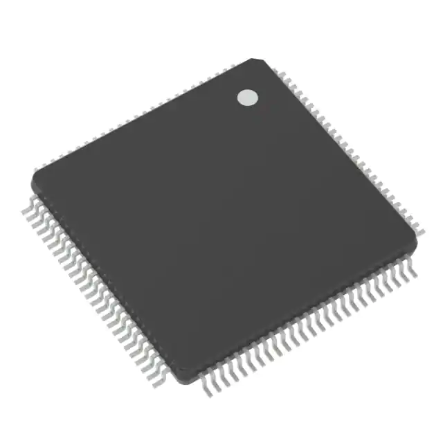
- Part No.:
- R5F56517EDFB#30
- Manufacturer:
- Renesas
- Category:
- Microcontrollers
- Package:
- 144-LQFP
- Datasheet:
-
 R5F56517EDFB#30.pdf
- Description:
- IC MCU 32BIT 768KB FLSH 144LFQFP
- Quantity:
- Payment:

- Shipping:

Inventory:240
Please send an inquiry. Send us your inquiry, and we will respond immediately.
Product details
Overview
R5F56517EDFB#30 from Renesas Electronics is a 32-bit RXv2 core MCU in LQFP-144 package, operating at up to 120 MHz with 2 MB flash, 384 KB RAM, and integrated USB 2.0 FS host/device, Ethernet MAC, and AES encryption engine - deployed as the main controller on the RX65N Envision Kit evaluation board.
For engineers reviewing the R5F56517EDFB#30 datasheet, R5F56517EDFB#30 pinout, R5F56517EDFB#30 application, or R5F56517EDFB#30 equivalent, key selection considerations include dual-bank flash architecture for secure firmware updates, hardware-based secure boot support, and integrated peripherals enabling rapid prototyping of industrial HMI and networked IoT edge nodes.
Technical Context
The R5F56517EDFB#30 implements Renesas' RXv2 CPU core with 2-stage pipeline, FPU, and 16-bit multiply-accumulate unit. It integrates a dedicated Secure Boot ROM and supports encrypted firmware loading via RSU files validated by SHA-256 and RSA-2048 signatures.
Firmware update operation relies on dual-bank flash (Bank A/B), bank-swap logic, and SW2-triggered 3-second hold for forced boot loader entry - enabling field-upgradable applications without external programming hardware.
Key Specifications
| Parameter | Value and Actual Design Meaning |
|---|---|
| CPU Core | RXv2 32-bit, 120 MHz max - enables real-time deterministic execution for industrial control loops. |
| Flash Memory | 2 MB dual-bank flash - supports atomic firmware updates with zero-downtime bank swapping. |
| RAM | 384 KB SRAM - sufficient for concurrent Ethernet TCP/IP stack, USB device stack, and GUI frame buffer. |
| Secure Boot | Hardware ROM-based boot loader with SHA-256/RSA-2048 validation - enforces firmware authenticity before execution. |
| USB Interface | USB 2.0 Full-Speed host/device - enables direct connection to USB memory sticks for RSU firmware loading. |
| Ethernet | 10/100 Mbps MAC with RMII interface - provides wired network connectivity for remote firmware deployment and diagnostics. |
Availability
R5F56517EDFB#30 is available at Aetrix Electronics and suitable for industrial HMI development, secure edge node prototyping, and Ethernet-connected embedded gateway design requiring stable component supply and long-term lifecycle support.
Supply support for R5F56517EDFB#30 includes scheduled delivery planning, volume procurement assistance, BOM continuity management, traceable sourcing, and lifecycle availability coordination for OEM customers, industrial embedded developers, connected-device designers, and electronics production programs.
Manufacturer
Renesas Electronics Corporation is a Japanese semiconductor manufacturer specializing in microcontrollers, analog, and power devices for automotive, industrial, and IoT applications.
The RX65N group - including R5F56517EDFB#30 - was designed for secure, networked human-machine interface applications with integrated crypto acceleration and dual-bank flash for robust over-the-air firmware updates.
FAQ
What is the role of R5F56517EDFB#30 on the RX65N Envision Kit?
R5F56517EDFB#30 serves as the primary application processor on the RX65N Envision Kit, executing preloaded demo firmware (std.rsu or bench.rsu) and managing USB-based firmware updates, touch display I/O, Ethernet communication, and secure boot verification. Its dual-bank flash and hardware crypto engine directly enable the kit's bank-swap update workflow.
How does R5F56517EDFB#30 support secure firmware updates?
R5F56517EDFB#30 uses an immutable Secure Boot ROM to validate RSU firmware images using SHA-256 hash and RSA-2048 signature checks before loading into flash. The dual-bank architecture allows verified firmware to be written to the inactive bank, then activated via atomic bank swap - ensuring no invalid firmware ever executes.
Which interfaces on R5F56517EDFB#30 are used for firmware loading from USB memory stick?
R5F56517EDFB#30 uses its integrated USB 2.0 Full-Speed peripheral in device mode to enumerate as a mass storage device during boot loader mode, and in host mode to read *.rsu files from USB memory sticks. SW2 hold detection triggers entry into this USB-host firmware loading state.
Does R5F56517EDFB#30 require external circuitry for Ethernet connectivity on the Envision Kit?
No - R5F56517EDFB#30 integrates a full 10/100 Mbps Ethernet MAC with RMII interface. On the RX65N Envision Kit, it connects directly to the LAN8720A PHY via RMII signals and MDC/MDIO lines; no external MAC or bridge IC is required for basic Ethernet operation.
Can R5F56517EDFB#30 execute benchmark and standard demos simultaneously?
No - R5F56517EDFB#30 runs only one active firmware image at a time, stored in either Bank A or Bank B. The boot loader selects which bank to execute at reset; switching between standard and benchmark demos requires a bank-swap operation followed by software reset, as implemented in the RX65N Envision Kit's update flow.
R5F56517EDFB#30 Specifications
- Product attributes
- Attribute value
- Manufacturer:
- Renesas
- Package/Case:
- 144-LQFP
- Series:
- RX651
- Packaging:
- Tray
- Product Status:
- Active
- Programmable:
- Not Verified
- Core Processor:
- RXv2
- Core Size:
- 32-Bit Single-Core
- Speed:
- 120MHz
- Connectivity:
- CANbus, EBI/EMI, Ethernet, I2C, LINbus, MMC/SD, QSPI, SCI, SPI, UART/USART, USB
- Peripherals:
- DMA, LVD, POR, PWM, WDT
- Number of I/O:
- 111
- Program Memory Size:
- 768KB (768K x 8)
- Program Memory Type:
- FLASH
- EEPROM Size:
- -
- RAM Size:
- 256K x 8
- Voltage - Supply (Vcc/Vdd):
- 2.7V ~ 3.6V
- Data Converters:
- A/D 29x12b; D/A 2x12b
- Oscillator Type:
- Internal
- Operating Temperature:
- -40°C ~ 85°C (TA)
- Grade:
- -
- Qualification:
- -
- Mounting Type:
- Surface Mount
- Supplier Device Package:
R5F56517EDFB#30 FAQ
1.How can I place an order for R5F56517EDFB#30 through Aetrix?
Please submit a Request for Quotation (RFQ) for R5F56517EDFB#30 on Aetrix. Our sales agent will provide a competitive quotation and guide you through the order confirmation once you accept the terms.
2.Are the price and stock information for R5F56517EDFB#30 reliable?
The price and inventory of R5F56517EDFB#30 are updated periodically and may fluctuate due to market conditions. Stock and pricing data are typically refreshed every 24 hours. Quotation validity for R5F56517EDFB#30 is usually 5 days.
3.What payment methods are accepted for R5F56517EDFB#30?
We accept Wire Transfer, PayPal, Credit Card, Western Union, MoneyGram, and Escrow for R5F56517EDFB#30 transactions.
Note: Certain payment methods may incur a processing fee.
4.How is shipping managed for R5F56517EDFB#30?
R5F56517EDFB#30 orders can be shipped via leading logistics carriers, including DHL, UPS, FedEx, TNT, or Registered Mail.
Once your R5F56517EDFB#30 order is processed, you will receive an email with the shipment details and tracking number.
Note: Tracking information may take up to 24 hours to appear. Express delivery typically takes 3–5 business days.
5.How can I obtain technical support or documentation for R5F56517EDFB#30?
For technical support, including R5F56517EDFB#30 datasheets, pinout diagrams, or application guidance, please contact our engineering support team. They can provide detailed documentation and assistance for your R5F56517EDFB#30 requirements.
6.How does Aetrix verify that R5F56517EDFB#30 is sourced from the original manufacturer or authorized distributors?
All R5F56517EDFB#30 products on Aetrix are procured from qualified distributors and authorized channels. Our dedicated quality assurance team conducts strict verification, including traceability checks and, if necessary, third-party testing. This ensures that R5F56517EDFB#30 meets industry standards.
7.What is the process for return or replacement of R5F56517EDFB#30?
All R5F56517EDFB#30 units undergo pre-shipment inspection (PSI). If there is an issue with R5F56517EDFB#30, returns or replacements are accepted under the following conditions:
1.Quantity discrepancies, incorrect items, or visible external defects (such as breakage or corrosion), acknowledged by Aetrix.
2.The issue is reported within 90 days of delivery.
3.The R5F56517EDFB#30 part is unused and in its original packaging.
Return procedure for R5F56517EDFB#30:
1.Submit a request within 90 days.
2.Obtain a Return Material Authorization (RMA) from Aetrix.
R5F56517EDFB#30 Tags

-
ATTINY4-TSHR
Microchip Technology
-
ATTINY10-TSHR
Microchip Technology
-
ATTINY10-TS8R
Microchip Technology

-
ATTINY202-SSNR
Microchip Technology
-
ATTINY202-SSFR
Microchip Technology
-
ATTINY402-SSNR
Microchip Technology

-
PIC16F15213T-I/MF
Microchip Technology
-
PIC16F15213-E/MF
Microchip Technology

-
PIC10F200T-I/OT
Microchip Technology
-
ATTINY412-SSNR
Microchip Technology
-
PIC10F202T-I/OT
Microchip Technology

-
ATTINY404-SSNR
Microchip Technology
Tech Hub

A practical engineering and sourcing framework covering lifecycle verification, lifetime-buy calculations, replacement qualification, supplier checks and counterfeit-risk controls.

TTL and CMOS logic families differ in thresholds, loading, output drive, power and timing. This engineering guide compares 74HC and 74HCT, calculates noise margins and checks 3.3 V/5 V compatibility.

A practical engineering guide to 3.3V and 5V logic compatibility, input thresholds, resistor dividers, translator ICs, MOSFET level shifting, I2C pull-ups, timing limits and power-sequencing risks.

The 74HC595 uses push-pull logic outputs, while the TPIC6B595 uses 50 V open-drain DMOS sinks for higher-power loads. This guide compares timing, current limits, 3.3 V interfacing, load wiring, thermal…

The 74HC595 converts serial data into eight stable parallel outputs. This guide covers pin functions, shift and storage timing, OE and MR behavior, drive-current limits, cascading, voltage compatibilit…

A technical comparison of level-sensitive latches and edge-triggered flip-flops, covering timing windows, setup and hold limits, master–slave operation, time borrowing, race-through, HDL inference and…

A D latch stores one bit while Enable controls when data can pass. This reference covers gate-level operation, truth tables, transparency, setup and hold timing, LE versus OE, common ICs and practical …

An SR latch stores one bit through cross-coupled feedback. This engineering reference covers NOR and NAND implementations, truth tables, forbidden-state recovery, gated operation, switch debouncing, fa…

Latch circuits retain one bit through feedback. This technical reference covers SR and D latches, truth tables, transparency, timing limits, latch-versus-flip-flop behavior, applications and common log…

An engineering guide to LED driver operation, constant-current and constant-voltage outputs, linear and switching topologies, dimming, IC selection, calculations, replacement compatibility, and fault c…


