
 My Inquiry
 My Account


Renesas R7F7016934AFP-C#KA1
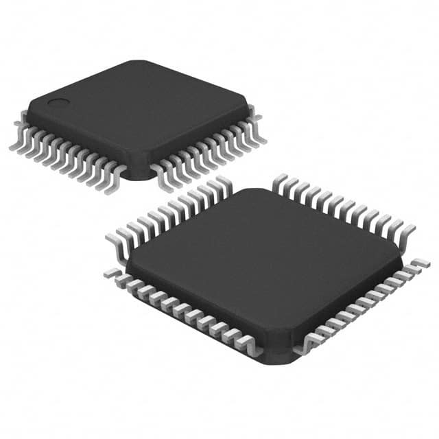
- Part No.:
- R7F7016934AFP-C#KA1
- Manufacturer:
- Renesas
- Category:
- Microcontrollers
- Package:
- 48-QFP
- Datasheet:
-
 R7F7016934AFP-C#KA1.pdf
- Description:
- IC MCU 32BIT 1MB FLASH 48LFQFP
- Quantity:
- Payment:

- Shipping:

Inventory:2,001
Please send an inquiry. Send us your inquiry, and we will respond immediately.
Product details
Overview
R7F7016934AFP-C#KA1 from Renesas Electronics is a 32-bit RH850/F1KH-D8 automotive microcontroller featuring dual-core lockstep CPU architecture, 4 MB on-chip flash memory, and ASIL-D compliance per ISO 26262 for safety-critical powertrain and chassis control applications. It integrates a 200 MHz core clock, 512 KB SRAM, and hardware safety mechanisms including ECC on flash/SRAM, BIST, and lockstep monitoring.
For engineers reviewing the R7F7016934AFP-C#KA1 datasheet, R7F7016934AFP-C#KA1 pinout, R7F7016934AFP-C#KA1 application, or R7F7016934AFP-C#KA1 equivalent, key selection considerations include its dual-lockstep execution mode, integrated CAN FD (up to 5 channels), Ethernet AVB support, and AEC-Q100 Grade 1 qualification for under-hood deployment.
Technical Context
The R7F7016934AFP-C#KA1 implements a dual-core RH850G3K-H CPU with hardware-enforced lockstep operation, where one core executes instructions while the other verifies results in real time. It supports full ASIL-D fault detection coverage via dedicated safety monitor logic, memory built-in self-test (MBIST), and flash ECC with error correction and notification.
It integrates multiple domain-specific peripherals: five CAN FD controllers with flexible data-rate support up to 5 Mbps, one 100BASE-T1 Ethernet AVB interface with time-sensitive networking (TSN) readiness, and a 12-bit SAR ADC with 48 channels and hardware trigger synchronization. All critical peripherals are safety-monitored and accessible via dedicated safety channels.
Key Specifications
| Parameter | Value and Actual Design Meaning |
|---|---|
| CPU Core | Dual RH850G3K-H cores in lockstep mode for ASIL-D compliance; no software redundancy required. |
| Max Clock Frequency | 200 MHz - enables deterministic real-time response for engine control loops with sub-1 µs interrupt latency. |
| Flash Memory | 4 MB with ECC, sector erase, and read-while-write capability - supports safe over-the-air (OTA) firmware updates. |
| SRAM | 512 KB with ECC and parity protection - ensures data integrity for safety-critical variables and stack operations. |
| CAN FD Interfaces | 5 independent channels supporting ISO 11898-1:2015, up to 5 Mbps data phase - suitable for high-bandwidth vehicle network domains. |
| Ethernet Interface | 1× 100BASE-T1 with AVB/TSN-ready MAC and integrated PHY - enables time-synchronized communication for ADAS sensor fusion. |
| ADC | 12-bit SAR with 48 input channels, hardware-triggered sampling, and window comparator - ideal for analog sensor monitoring in powertrain systems. |
Pinout & Package
Package: 176-pin LQFP (24 mm × 24 mm, 0.5 mm pitch), AEC-Q100 Grade 1 qualified for operation from −40°C to +125°C ambient.
| Pin/Terminal | Circuit Role | Design Meaning |
|---|---|---|
| VDDP1–VDDP8 | Core Power Supply | Eight independent 1.2 V supplies for CPU, peripherals, and safety logic - enable localized fault isolation and power domain control. |
| VSSP1–VSSP8 | Core Ground | Dedicated ground returns matching each VDDP pin - minimize noise coupling between functional blocks. |
| CLKIN / CLKOUT | External Clock Input/Output | Supports crystal or oscillator input (1–20 MHz); CLKOUT provides buffered system clock for trace/debug or external sync. |
| RESETn | Active-Low Reset Input | Asynchronous reset with internal pull-up; initiates full safety initialization sequence including BIST and ECC scrubbing. |
| TRSTn / TDI / TDO / TMS / TCK | JTAG Debug Interface | Fully compliant IEEE 1149.1; supports boundary scan, debug access, and safety verification during production test. |
| CANFD0_TX / CANFD0_RX | CAN FD Channel 0 I/O | Differential transceiver pins supporting 1–5 Mbps data rate; integrated termination resistors configurable via register. |
| ETH_MII_TXD0–TXD3 / ETH_MII_TX_EN / ETH_MII_TX_CLK | Ethernet MII Transmit Signals | 100 Mbps MII interface signals - connect directly to external 100BASE-T1 PHY without level-shifting. |
Key Features
| Feature | Design Value |
|---|---|
| Hardware Lockstep CPU | Dual-core execution with cycle-accurate comparison eliminates need for software-based safety checks in ASIL-D paths. |
| Integrated Safety Monitor | Dedicated safety controller performs runtime monitoring of clock frequency, voltage, temperature, and memory integrity - triggers fail-safe state on violation. |
| Flash ECC & Repair | Single-bit error correction and double-bit error detection with automatic repair on read - prevents silent data corruption in boot code and calibration tables. |
| Flexible Peripheral Clock Gating | Independent clock enables per peripheral group - reduces dynamic power by >40% during low-duty-cycle sensor polling. |
| Secure Boot with ROM-based Public Key Verification | Immutable boot ROM validates signed firmware images using ECDSA P-256 before execution - prevents unauthorized code injection. |
Applications
| Engine Control Unit (ECU) | Electric Power Steering (EPS) |
|---|---|
|
Use Scenario: Real-time combustion timing, fuel injection, and knock control in gasoline/diesel engines under transient load conditions. IC Role / Device Role / Timing Role: Primary ASIL-D safety controller executing closed-loop control algorithms with <100 µs jitter tolerance. Use Value: Dual-lockstep execution and hardware BIST ensure deterministic behavior and zero latent faults in torque calculation paths. |
Use Scenario: Torque assist computation, motor position feedback processing, and fail-operational steering fallback in EPS systems. IC Role / Device Role / Timing Role: Safety-certified host MCU managing motor control loop (PWM generation), CAN FD communication, and torque sensor fusion. Use Value: Integrated 5-channel CAN FD and hardware ADC trigger synchronization reduce external component count and interconnect failure modes. |
| Brake-by-Wire System | Vehicle Domain Controller (VDC) |
|
Use Scenario: Redundant hydraulic pressure modulation and brake actuator supervision in electro-hydraulic brake systems. IC Role / Device Role / Timing Role: ASIL-D certified controller performing dual-channel pressure control with cross-monitoring and diagnostic reporting. Use Value: ECC-protected SRAM and lockstep CPU guarantee integrity of critical braking commands even under single-point hardware faults. |
Use Scenario: Centralized coordination of ADAS sensors, gateway functions, and OTA update orchestration across vehicle domains. IC Role / Device Role / Timing Role: High-integration domain MCU hosting Ethernet AVB for camera/LiDAR streaming and CAN FD for legacy ECU bridging. Use Value: 100BASE-T1 Ethernet + 5× CAN FD enables scalable, time-synchronized domain architecture without external bridge ICs. |
Equivalent & Alternatives
The following parts are listed as comparable options for similar automotive safety MCU applications.
| Alternative Part | Technical Difference | Application Difference | Selection Advice |
|---|---|---|---|
| R7F7016924AFP-C#KA1 | Same RH850/F1KH-D8 family, but with 2 MB flash and 256 KB SRAM - reduced memory capacity and lower cost. | Suitable for mid-tier powertrain modules where OTA update size and calibration table depth are constrained. | Select when full 4 MB flash is not required and BOM cost sensitivity outweighs future scalability needs. |
| TC397XP-128F300S-DC | Infineon AURIX™ TC397 with TriCore™ V1.6.2, 300 MHz, 8 MB flash, but single-core lockstep (not dual-core). | Offers higher clock speed and larger memory, but uses different safety architecture (lockstep vs. dual-core verification). | Choose for applications requiring higher computational throughput and established AURIX toolchain compatibility, accepting architectural divergence. |
Compared with R7F7016934AFP-C#KA1, the R7F7016924AFP-C#KA1 reduces memory resources for cost-sensitive deployments, while the TC397XP-128F300S-DC provides greater raw performance and ecosystem maturity at the expense of differing safety implementation and vendor toolchain alignment.
Availability
R7F7016934AFP-C#KA1 is available at Aetrix Electronics and suitable for engine control units, electric power steering systems, brake-by-wire modules, and vehicle domain controllers requiring stable component supply across multi-year automotive production cycles.
Supply support for R7F7016934AFP-C#KA1 includes scheduled delivery planning, volume procurement assistance, BOM continuity management, traceable sourcing, and lifecycle availability coordination for OEM customers, industrial embedded developers, connected-device designers, and electronics production programs.
Manufacturer
Renesas Electronics Corporation is a Japanese semiconductor manufacturer specializing in microcontrollers, analog, and power devices for automotive, industrial, and infrastructure markets.
The RH850/F1KH product line delivers ASIL-D capable MCUs for powertrain and chassis control, designed specifically to meet ISO 26262 requirements with integrated hardware safety features and automotive-grade reliability.
FAQ
What is the safety certification status of the R7F7016934AFP-C#KA1?
The R7F7016934AFP-C#KA1 is certified to ASIL D per ISO 26262:2018 for hardware elements and supports ASIL D software development when used with Renesas' certified safety manual and diagnostic software library. Its dual-lockstep CPU, ECC memory, and integrated safety monitor are all validated for use in safety-critical powertrain applications. The R7F7016934AFP-C#KA1 meets AEC-Q100 Grade 1 requirements for operation from −40°C to +125°C.
Does the R7F7016934AFP-C#KA1 support over-the-air (OTA) firmware updates?
Yes, the R7F7016934AFP-C#KA1 supports secure OTA updates through its 4 MB flash memory with read-while-write capability and hardware-accelerated cryptographic functions. The boot ROM enforces ECDSA signature verification before loading new firmware, and flash ECC ensures integrity during write/erase cycles. This allows safe field updates without compromising ASIL-D compliance of the R7F7016934AFP-C#KA1.
How many CAN FD interfaces does the R7F7016934AFP-C#KA1 integrate?
The R7F7016934AFP-C#KA1 integrates five independent CAN FD controllers compliant with ISO 11898-1:2015, each supporting data rates up to 5 Mbps in the data phase. These interfaces feature configurable bit timing, hardware message filtering, and dedicated DMA channels - enabling high-bandwidth communication across multiple vehicle domains without external CAN transceivers beyond physical layer drivers.
What is the maximum operating temperature range for the R7F7016934AFP-C#KA1?
The R7F7016934AFP-C#KA1 is qualified to AEC-Q100 Grade 1, supporting continuous operation from −40°C to +125°C ambient temperature. This rating is verified across all electrical parameters and safety mechanisms, making the R7F7016934AFP-C#KA1 suitable for under-hood applications such as engine control and transmission control units where thermal stress is severe.
Is Ethernet AVB supported natively on the R7F7016934AFP-C#KA1?
Yes, the R7F7016934AFP-C#KA1 includes a native 100BASE-T1 Ethernet MAC with AVB/TSN-ready features, including timestamping, traffic shaping, and gate control list support. It interfaces directly with standard 100BASE-T1 PHYs and requires no external bridge ICs. This enables time-deterministic communication for ADAS sensor fusion and domain controller applications using the R7F7016934AFP-C#KA1.
R7F7016934AFP-C#KA1 Specifications
- Product attributes
- Attribute value
- Manufacturer:
- Renesas
- Package/Case:
- 48-QFP
- Series:
- RH850/F1KM-S1
- Packaging:
- Tape & Reel (TR)
- Product Status:
- Active
- Programmable:
- Not Verified
- Core Processor:
- RH850G3KH
- Core Size:
- 32-Bit Single-Core
- Speed:
- 120MHz
- Connectivity:
- CANbus, CSI, I2C, LINbus, SPI, UART/USART
- Peripherals:
- DMA, PWM, WDT
- Number of I/O:
- 33
- Program Memory Size:
- 1MB (1M x 8)
- Program Memory Type:
- FLASH
- EEPROM Size:
- 64K x 8
- RAM Size:
- 128K x 8
- Voltage - Supply (Vcc/Vdd):
- 3V ~ 5.5V
- Data Converters:
- A/D 4x10b, 8x12b
- Oscillator Type:
- Internal
- Operating Temperature:
- -40°C ~ 125°C (TA)
- Grade:
- Automotive
- Qualification:
- AEC-Q100
- Mounting Type:
- Surface Mount
- Supplier Device Package:
R7F7016934AFP-C#KA1 FAQ
1.How can I place an order for R7F7016934AFP-C#KA1 through Aetrix?
Please submit a Request for Quotation (RFQ) for R7F7016934AFP-C#KA1 on Aetrix. Our sales agent will provide a competitive quotation and guide you through the order confirmation once you accept the terms.
2.Are the price and stock information for R7F7016934AFP-C#KA1 reliable?
The price and inventory of R7F7016934AFP-C#KA1 are updated periodically and may fluctuate due to market conditions. Stock and pricing data are typically refreshed every 24 hours. Quotation validity for R7F7016934AFP-C#KA1 is usually 5 days.
3.What payment methods are accepted for R7F7016934AFP-C#KA1?
We accept Wire Transfer, PayPal, Credit Card, Western Union, MoneyGram, and Escrow for R7F7016934AFP-C#KA1 transactions.
Note: Certain payment methods may incur a processing fee.
4.How is shipping managed for R7F7016934AFP-C#KA1?
R7F7016934AFP-C#KA1 orders can be shipped via leading logistics carriers, including DHL, UPS, FedEx, TNT, or Registered Mail.
Once your R7F7016934AFP-C#KA1 order is processed, you will receive an email with the shipment details and tracking number.
Note: Tracking information may take up to 24 hours to appear. Express delivery typically takes 3–5 business days.
5.How can I obtain technical support or documentation for R7F7016934AFP-C#KA1?
For technical support, including R7F7016934AFP-C#KA1 datasheets, pinout diagrams, or application guidance, please contact our engineering support team. They can provide detailed documentation and assistance for your R7F7016934AFP-C#KA1 requirements.
6.How does Aetrix verify that R7F7016934AFP-C#KA1 is sourced from the original manufacturer or authorized distributors?
All R7F7016934AFP-C#KA1 products on Aetrix are procured from qualified distributors and authorized channels. Our dedicated quality assurance team conducts strict verification, including traceability checks and, if necessary, third-party testing. This ensures that R7F7016934AFP-C#KA1 meets industry standards.
7.What is the process for return or replacement of R7F7016934AFP-C#KA1?
All R7F7016934AFP-C#KA1 units undergo pre-shipment inspection (PSI). If there is an issue with R7F7016934AFP-C#KA1, returns or replacements are accepted under the following conditions:
1.Quantity discrepancies, incorrect items, or visible external defects (such as breakage or corrosion), acknowledged by Aetrix.
2.The issue is reported within 90 days of delivery.
3.The R7F7016934AFP-C#KA1 part is unused and in its original packaging.
Return procedure for R7F7016934AFP-C#KA1:
1.Submit a request within 90 days.
2.Obtain a Return Material Authorization (RMA) from Aetrix.
R7F7016934AFP-C#KA1 Tags

-
ATTINY4-TSHR
Microchip Technology
-
ATTINY10-TSHR
Microchip Technology
-
ATTINY10-TS8R
Microchip Technology

-
ATTINY202-SSNR
Microchip Technology
-
ATTINY202-SSFR
Microchip Technology
-
ATTINY402-SSNR
Microchip Technology

-
PIC16F15213T-I/MF
Microchip Technology
-
PIC16F15213-E/MF
Microchip Technology

-
PIC10F200T-I/OT
Microchip Technology
-
ATTINY412-SSNR
Microchip Technology
-
PIC10F202T-I/OT
Microchip Technology

-
ATTINY404-SSNR
Microchip Technology
Tech Hub

TTL and CMOS logic families differ in thresholds, loading, output drive, power and timing. This engineering guide compares 74HC and 74HCT, calculates noise margins and checks 3.3 V/5 V compatibility.

A practical engineering guide to 3.3V and 5V logic compatibility, input thresholds, resistor dividers, translator ICs, MOSFET level shifting, I2C pull-ups, timing limits and power-sequencing risks.

The 74HC595 uses push-pull logic outputs, while the TPIC6B595 uses 50 V open-drain DMOS sinks for higher-power loads. This guide compares timing, current limits, 3.3 V interfacing, load wiring, thermal…

The 74HC595 converts serial data into eight stable parallel outputs. This guide covers pin functions, shift and storage timing, OE and MR behavior, drive-current limits, cascading, voltage compatibilit…

A technical comparison of level-sensitive latches and edge-triggered flip-flops, covering timing windows, setup and hold limits, master–slave operation, time borrowing, race-through, HDL inference and…

A D latch stores one bit while Enable controls when data can pass. This reference covers gate-level operation, truth tables, transparency, setup and hold timing, LE versus OE, common ICs and practical …

An SR latch stores one bit through cross-coupled feedback. This engineering reference covers NOR and NAND implementations, truth tables, forbidden-state recovery, gated operation, switch debouncing, fa…

Latch circuits retain one bit through feedback. This technical reference covers SR and D latches, truth tables, transparency, timing limits, latch-versus-flip-flop behavior, applications and common log…

An engineering guide to LED driver operation, constant-current and constant-voltage outputs, linear and switching topologies, dimming, IC selection, calculations, replacement compatibility, and fault c…

Operational amplifier guide covering op amp basics, feedback, ideal vs real op amps, common configurations, buffer circuits, offset, bias current, gain-bandwidth, slew rate, rail-to-rail limits and sel…


