
 My Inquiry
 My Account


Renesas R7S721020VCFP#AA1
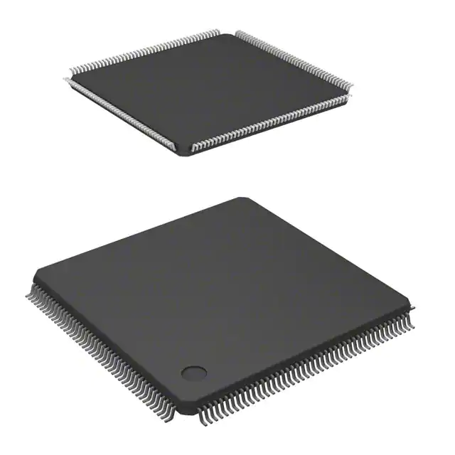
- Part No.:
- R7S721020VCFP#AA1
- Manufacturer:
- Renesas
- Category:
- Microprocessors
- Package:
- 176-LQFP
- Datasheet:
-
 R7S721020VCFP#AA1.pdf
- Description:
- IC MPU RZ/A1L 400MHZ 176LFQFP
- Quantity:
- Payment:

- Shipping:

Inventory:4,158
Please send an inquiry. Send us your inquiry, and we will respond immediately.
Product details
Overview
R7S721020VCFP#AA1 from Renesas Electronics is a high-performance 32-bit ARM Cortex-A9 microprocessor in the RZ/A1L Group, integrating 10 MB on-chip SRAM, dual-channel DDR2/DDR3 SDRAM controller, and hardware-accelerated 2D graphics engine. It operates at up to 400 MHz, supports Linux and Android OS, and targets embedded HMI applications requiring rich GUI, real-time responsiveness, and low-power operation.
For engineers reviewing the R7S721020VCFP#AA1 datasheet, R7S721020VCFP#AA1 pinout, R7S721020VCFP#AA1 application, or R7S721020VCFP#AA1 equivalent, key selection criteria include its integrated SRAM size, DDR interface compatibility, boot source flexibility (SPI flash, SD, USB), and support for industrial temperature range (–40°C to +85°C) without external memory.
Technical Context
The R7S721020VCFP#AA1 implements a dual-core capable Cortex-A9 CPU with NEON and VFPv4 extensions, coupled with a tightly coupled 10 MB SRAM block accessible as L2 cache or system memory. Its memory subsystem includes configurable AXI bus interconnect, remappable address space, and hardware-assisted memory protection unit (MPU).
Boot configuration is determined by dedicated mode pins (MD0–MD3), supporting four distinct boot sources including serial flash, SD card, USB host, and JTAG. Clock generation uses a programmable PLL with fractional divider, enabling precise frequency synthesis for DDR, AXI, and peripheral clocks while supporting spread-spectrum clocking (SSCG) for EMI reduction.
Key Specifications
| Parameter | Value and Actual Design Meaning |
|---|---|
| CPU Core | ARM Cortex-A9, single-core, 400 MHz max - enables Linux-based HMI with deterministic interrupt latency |
| On-chip Memory | 10 MB SRAM - eliminates need for external SDRAM in many GUI applications, reducing BOM and PCB area |
| Memory Interface | DDR2/DDR3 SDRAM controller (16-bit, 400 MHz) - supports cost-optimized external memory for high-bandwidth display buffers |
| Graphics Acceleration | 2D graphics engine (Renesas GC320) - offloads GUI rendering, freeing CPU for application logic and communication tasks |
| Operating Temp | –40°C to +85°C - qualified for industrial and automotive cabin HMI environments without derating |
| Package | FCBGA-324, 15 mm × 15 mm, 0.65 mm pitch - compatible with standard reflow profiles and automated optical inspection |
| Power Supply | Core: 1.0 V ±3%; I/O: 1.8 V/3.3 V selectable - simplifies power tree design with minimal voltage rails |
Pinout & Package
Package: Fine-pitch Flip-Chip Ball Grid Array (FCBGA) with 324 solder balls, 15 mm × 15 mm body, 0.65 mm ball pitch, and Pb-free/NiPdAu surface finish per JEDEC J-STD-020.
| Pin/Terminal | Circuit Role | Design Meaning |
|---|---|---|
| VDDCORE | Core power supply | 1.0 V input for CPU, cache, and internal logic; requires low-noise regulation and local decoupling |
| VDDIO_1P8 / VDDIO_3P3 | I/O power supply | Selectable 1.8 V or 3.3 V rail for all GPIOs and peripheral interfaces; configured at boot |
| CLKIN | Main clock input | Accepts 12–24 MHz crystal or external clock; feeds PLL for system clock generation |
| RESET_N | Active-low reset input | Synchronous deassertion required after power stabilization and clock lock; drives internal POR circuit |
| MD0–MD3 | Boot mode select | Hardwired pull-up/down at power-on to define boot source (SPI, SD, USB, JTAG) |
| SDA/SCL | I²C bus interface | Dedicated pins for system management EEPROM, PMIC control, or touch controller communication |
Key Features
| Feature | Design Value |
|---|---|
| Integrated 10 MB SRAM | Eliminates external DRAM in GUI applications, reducing bill-of-materials cost and improving boot time reliability |
| Hardware 2D Graphics Engine (GC320) | Accelerates bitblt, alpha blending, and rotation operations at >100 MPixels/s, enabling smooth 800×480 displays |
| Flexible Boot Options | Supports SPI NOR flash, SD card, USB host, and JTAG - enables field firmware updates and secure provisioning |
| Dual-Voltage I/O Banks | Independent 1.8 V/3.3 V selection per bank allows direct interfacing with legacy and modern peripherals without level shifters |
| AXI Bus Remapping | Runtime-configurable address map enables dynamic memory partitioning between application code, graphics buffer, and DMA descriptors |
Applications
| Industrial HMI Panel | Medical Device Display |
|---|---|
Use Scenario: Touch-enabled operator interface for PLC-controlled machinery with real-time status visualization and alarm logging. IC Role / Device Role / Timing Role: Main application processor executing Linux, managing display refresh (60 Hz), handling CAN/Ethernet comms, and running safety-critical UI logic. Use Value: On-chip 10 MB SRAM ensures deterministic frame buffer access; hardware GC320 enables responsive touch feedback without CPU load spikes. | Use Scenario: Portable diagnostic device with color LCD, battery monitoring, and wireless data upload via Wi-Fi module. IC Role / Device Role / Timing Role: System-on-chip processor running Android framework, driving 480×800 TFT, managing USB OTG for firmware update, and coordinating sensor data acquisition. Use Value: Single-chip integration reduces board area and power consumption; industrial temp grade supports operation in uncontrolled clinical environments. |
| Automotive Infotainment Terminal | Smart Building Control Gateway |
Use Scenario: Cabin-mounted infotainment unit with audio playback, Bluetooth hands-free, and vehicle telemetry display. IC Role / Device Role / Timing Role: Application processor executing QNX/Linux, synchronizing audio clock (I²S), decoding MP3/AAC, and rendering navigation overlays. Use Value: DDR controller supports dual-channel video/audio buffers; SSCG reduces EMI in sensitive RF bands near cellular modules. | Use Scenario: Wall-mounted HVAC and lighting controller with web-based configuration, Zigbee/Thread radio coexistence, and local history logging. IC Role / Device Role / Timing Role: Central controller managing multiple RTOS tasks, Ethernet/Wi-Fi stack, secure TLS handshake, and real-time sensor polling. Use Value: Hardware crypto acceleration (AES-128/SHA-1) secures OTA updates; flexible boot enables signed firmware validation from SPI flash. |
Equivalent & Alternatives
The following parts are listed as comparable options for similar microprocessor applications.
| Alternative Part | Technical Difference | Application Difference | Selection Advice |
|---|---|---|---|
| R7S721030VCFP#AA1 | Same RZ/A1L family, but with 16 MB on-chip SRAM and identical pinout | Preferred where larger frame buffers or multi-app Linux environments require >10 MB contiguous memory | Select when GUI complexity demands extra SRAM headroom; no PCB change needed |
| R7S721010VCFP#AA1 | Same package and core, but only 5 MB on-chip SRAM and no GC320 graphics engine | Suitable for text-only HMIs or headless control applications without display acceleration | Choose for cost-sensitive designs where graphics acceleration is unnecessary |
Compared with R7S721020VCFP#AA1, the R7S721030VCFP#AA1 offers higher SRAM capacity for richer GUIs, while the R7S721010VCFP#AA1 trades graphics capability and memory for lower unit cost - all three share identical footprint, boot architecture, and peripheral set.
Availability
R7S721020VCFP#AA1 is available at Aetrix Electronics and suitable for industrial HMI panels, medical display terminals, automotive infotainment units, and smart building gateways requiring stable component supply across multi-year production cycles.
Supply support for R7S721020VCFP#AA1 includes scheduled delivery planning, volume procurement assistance, BOM continuity management, traceable sourcing, and lifecycle availability coordination for OEM customers, industrial embedded developers, connected-device designers, and electronics production programs.
Manufacturer
Renesas Electronics Corporation is a Japanese semiconductor manufacturer specializing in microcontrollers, microprocessors, analog, and power devices for industrial, automotive, and enterprise applications.
The RZ/A series, including R7S721020VCFP#AA1, was designed to deliver Linux-capable application processing with integrated memory and graphics for resource-constrained embedded HMI systems - eliminating external DRAM and reducing system-level complexity.
FAQ
What operating systems are officially supported on the R7S721020VCFP#AA1?
R7S721020VCFP#AA1 is officially supported with Linux (Yocto Project v2.2+), Android 6.0+, and FreeRTOS. Renesas provides Board Support Packages (BSPs), kernel drivers, and graphics libraries (eGFX) specifically validated for R7S721020VCFP#AA1. The 10 MB on-chip SRAM enables full Linux boot without external DRAM in minimal configurations, and the GC320 engine is fully integrated into the DRM/KMS display subsystem.
Does the R7S721020VCFP#AA1 require an external DDR memory chip?
R7S721020VCFP#AA1 does not require external DDR memory for basic operation due to its integrated 10 MB SRAM, which can serve as main memory for Linux or RTOS applications with modest footprint. However, external DDR2/DDR3 is required for high-resolution display buffers, multimedia decoding, or multi-process workloads exceeding 10 MB. The DDR controller supports 16-bit bus width and up to 400 MHz data rate, and R7S721020VCFP#AA1's pinout includes dedicated DQ/DQS/DM signals for this interface.
What boot sources does the R7S721020VCFP#AA1 support, and how are they selected?
R7S721020VCFP#AA1 supports four boot modes selected by MD0–MD3 pins at power-on: SPI flash (Mode 0), SD card (Mode 1), USB host (Mode 2), and JTAG debug (Mode 3). Each mode defines the initial vector fetch location and initializes corresponding peripheral controllers. For example, Mode 0 configures the SPI interface to load bootloader from a 4-byte-addressable NOR flash, while Mode 2 activates USB PHY and enumeration logic to accept firmware image from a host PC. All modes retain access to on-chip ROM bootloader and security features like secure boot signature verification.
How is graphics acceleration implemented in the R7S721020VCFP#AA1?
R7S721020VCFP#AA1 integrates the Renesas GC320 2D graphics engine, a fixed-function hardware block supporting bitblt, alpha blending, color conversion (RGB/YUV), and rotation/scaling of rectangular regions. It operates independently of the Cortex-A9 CPU, using dedicated AXI master port to access frame buffers in SRAM or DDR. Driver support is provided through eGFX API and DRM/KMS integration, enabling direct rendering to display pipelines without CPU intervention - critical for achieving consistent 60 Hz refresh on 800×480 panels using R7S721020VCFP#AA1.
What thermal and power specifications apply to the R7S721020VCFP#AA1 in industrial applications?
R7S721020VCFP#AA1 is rated for industrial temperature range (–40°C to +85°C) and specifies typical power consumption of 1.2 W at 400 MHz with 10 MB SRAM active and DDR interface idle. Power delivery requires separate 1.0 V core and 1.8 V/3.3 V I/O supplies, each with defined ripple limits (±30 mV for VDDCORE). Thermal design must accommodate 12.5 W/m²·K junction-to-case resistance in FCBGA-324 package; Renesas recommends 4-layer PCB with internal ground/power planes and ≥4 thermal vias under the package center for convection-cooled industrial enclosures using R7S721020VCFP#AA1.
R7S721020VCFP#AA1 Specifications
- Product attributes
- Attribute value
- Manufacturer:
- Renesas
- Package/Case:
- 176-LQFP
- Series:
- RZ/A1L
- Packaging:
- Tray
- Product Status:
- Active
- Core Processor:
- ARM® Cortex®-A9
- Number of Cores/Bus Width:
- 1 Core, 32-Bit
- Speed:
- 400MHz
- Co-Processors/DSP:
- Multimedia; NEON™ MPE
- RAM Controllers:
- SDRAM, SRAM
- Graphics Acceleration:
- Yes
- Display & Interface Controllers:
- VDC
- Ethernet:
- 10/100Mbps
- SATA:
- -
- USB:
- USB 2.0 (2)
- Voltage - I/O:
- 1.2V, 3.3V
- Operating Temperature:
- -40°C ~ 85°C (TA)
- Grade:
- -
- Qualification:
- -
- Security Features:
- -
- Mounting Type:
- Surface Mount
- Supplier Device Package:
- 176-LFQFP (24x24)
- Additional Interfaces:
- CAN, I2C, IEBus, IrDA, LIN, MediaLB, MMC/SD/SDIO, SCI, SCI FIFO, SPDIF, SPI, SSI
R7S721020VCFP#AA1 FAQ
1.How can I place an order for R7S721020VCFP#AA1 through Aetrix?
Please submit a Request for Quotation (RFQ) for R7S721020VCFP#AA1 on Aetrix. Our sales agent will provide a competitive quotation and guide you through the order confirmation once you accept the terms.
2.Are the price and stock information for R7S721020VCFP#AA1 reliable?
The price and inventory of R7S721020VCFP#AA1 are updated periodically and may fluctuate due to market conditions. Stock and pricing data are typically refreshed every 24 hours. Quotation validity for R7S721020VCFP#AA1 is usually 5 days.
3.What payment methods are accepted for R7S721020VCFP#AA1?
We accept Wire Transfer, PayPal, Credit Card, Western Union, MoneyGram, and Escrow for R7S721020VCFP#AA1 transactions.
Note: Certain payment methods may incur a processing fee.
4.How is shipping managed for R7S721020VCFP#AA1?
R7S721020VCFP#AA1 orders can be shipped via leading logistics carriers, including DHL, UPS, FedEx, TNT, or Registered Mail.
Once your R7S721020VCFP#AA1 order is processed, you will receive an email with the shipment details and tracking number.
Note: Tracking information may take up to 24 hours to appear. Express delivery typically takes 3–5 business days.
5.How can I obtain technical support or documentation for R7S721020VCFP#AA1?
For technical support, including R7S721020VCFP#AA1 datasheets, pinout diagrams, or application guidance, please contact our engineering support team. They can provide detailed documentation and assistance for your R7S721020VCFP#AA1 requirements.
6.How does Aetrix verify that R7S721020VCFP#AA1 is sourced from the original manufacturer or authorized distributors?
All R7S721020VCFP#AA1 products on Aetrix are procured from qualified distributors and authorized channels. Our dedicated quality assurance team conducts strict verification, including traceability checks and, if necessary, third-party testing. This ensures that R7S721020VCFP#AA1 meets industry standards.
7.What is the process for return or replacement of R7S721020VCFP#AA1?
All R7S721020VCFP#AA1 units undergo pre-shipment inspection (PSI). If there is an issue with R7S721020VCFP#AA1, returns or replacements are accepted under the following conditions:
1.Quantity discrepancies, incorrect items, or visible external defects (such as breakage or corrosion), acknowledged by Aetrix.
2.The issue is reported within 90 days of delivery.
3.The R7S721020VCFP#AA1 part is unused and in its original packaging.
Return procedure for R7S721020VCFP#AA1:
1.Submit a request within 90 days.
2.Obtain a Return Material Authorization (RMA) from Aetrix.
R7S721020VCFP#AA1 Tags

-
AT91SAM9260B-CU-999
Microchip Technology
-
AT91SAM9G25-CU
Microchip Technology

-
ATSAMA5D27C-CU
Microchip Technology
-
AT91SAM9X35-CU
Microchip Technology
-
AT91SAM9X25-CU
Microchip Technology

-
MCIMX6Y2CVM08AB
NXP Semiconductors
.JPG)
-
AM3352BZCZ100
Texas Instruments
-
AT91SAM9260B-CU
Microchip Technology

-
AT91SAM9260B-QU
Microchip Technology

-
ATSAMA5D31A-CU
Microchip Technology
-
AT91SAM9G20B-CU-999
Microchip Technology
-
MCIMX6Y2CVM05AB
NXP Semiconductors
Tech Hub

TTL and CMOS logic families differ in thresholds, loading, output drive, power and timing. This engineering guide compares 74HC and 74HCT, calculates noise margins and checks 3.3 V/5 V compatibility.

A practical engineering guide to 3.3V and 5V logic compatibility, input thresholds, resistor dividers, translator ICs, MOSFET level shifting, I2C pull-ups, timing limits and power-sequencing risks.

The 74HC595 uses push-pull logic outputs, while the TPIC6B595 uses 50 V open-drain DMOS sinks for higher-power loads. This guide compares timing, current limits, 3.3 V interfacing, load wiring, thermal…

The 74HC595 converts serial data into eight stable parallel outputs. This guide covers pin functions, shift and storage timing, OE and MR behavior, drive-current limits, cascading, voltage compatibilit…

A technical comparison of level-sensitive latches and edge-triggered flip-flops, covering timing windows, setup and hold limits, master–slave operation, time borrowing, race-through, HDL inference and…

A D latch stores one bit while Enable controls when data can pass. This reference covers gate-level operation, truth tables, transparency, setup and hold timing, LE versus OE, common ICs and practical …

An SR latch stores one bit through cross-coupled feedback. This engineering reference covers NOR and NAND implementations, truth tables, forbidden-state recovery, gated operation, switch debouncing, fa…

Latch circuits retain one bit through feedback. This technical reference covers SR and D latches, truth tables, transparency, timing limits, latch-versus-flip-flop behavior, applications and common log…

An engineering guide to LED driver operation, constant-current and constant-voltage outputs, linear and switching topologies, dimming, IC selection, calculations, replacement compatibility, and fault c…

Operational amplifier guide covering op amp basics, feedback, ideal vs real op amps, common configurations, buffer circuits, offset, bias current, gain-bandwidth, slew rate, rail-to-rail limits and sel…


