
 My Inquiry
 My Account


Renesas R7S721020VLFP#AA1
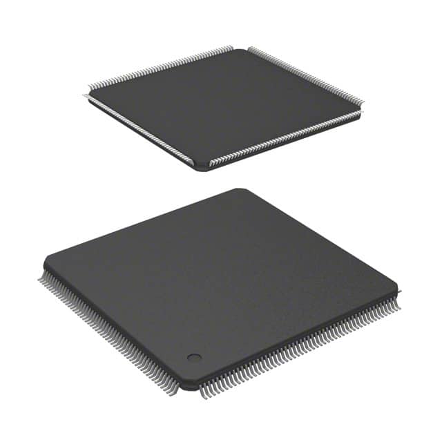
- Part No.:
- R7S721020VLFP#AA1
- Manufacturer:
- Renesas
- Category:
- Microprocessors
- Package:
- 176-LQFP
- Datasheet:
-
 R7S721020VLFP#AA1.pdf
- Description:
- IC MPU RZ/A1L 400MHZ 176LFQFP
- Quantity:
- Payment:

- Shipping:

Inventory:3,412
Please send an inquiry. Send us your inquiry, and we will respond immediately.
Product details
Overview
R7S721020VLFP#AA1 from Renesas Electronics is a high-performance 32-bit ARM Cortex-A9 microprocessor unit (MPU) in the RZ/A1L Group, featuring 512 KB L2 cache, integrated DRAM controller (LPDDR2/LPDDR3), and dual USB 2.0 host/device interfaces. It targets embedded human-machine interface (HMI) applications requiring rich graphics, real-time responsiveness, and secure boot.
For engineers reviewing the R7S721020VLFP#AA1 datasheet, R7S721020VLFP#AA1 pinout, R7S721020VLFP#AA1 application, or R7S721020VLFP#AA1 equivalent, key selection criteria include LPDDR2/3 memory interface support, 24-bit RGB parallel LCD controller, hardware-accelerated 2D graphics (CG2D), TrustZone-enabled secure boot, and industrial temperature grade (–40°C to +85°C) operation.
Technical Context
The R7S721020VLFP#AA1 implements a dual-core ARM Cortex-A9 MPCore CPU with NEON and VFPv4 extensions, coupled with a 512 KB unified L2 cache and on-chip SRAM (128 KB). Its memory subsystem supports LPDDR2-1066 and LPDDR3-1600 via a 32-bit bus with ECC protection for critical code/data regions.
System-level integration includes a 24-bit RGB parallel LCD controller with alpha blending, two independent USB 2.0 OTG controllers (one with PHY, one requiring external PHY), and a full-featured interrupt controller supporting 128 IRQ sources with priority nesting and vectoring. Clock management uses a multi-stage PLL system with programmable dividers for precise domain-specific frequency synthesis.
Key Specifications
| Parameter | Value and Actual Design Meaning |
|---|---|
| CPU Core | ARM Cortex-A9 dual-core @ up to 600 MHz; enables concurrent OS and application execution with deterministic latency. |
| L2 Cache | 512 KB unified; reduces external memory bandwidth pressure and improves real-time response for HMI rendering tasks. |
| Memory Interface | 32-bit LPDDR2/LPDDR3 @ 1066/1600 Mbps; supports low-power, high-bandwidth graphics frame buffer access without external SDRAM controller. |
| Graphics Acceleration | CG2D hardware engine; offloads 2D bitblt, alpha blending, and rotation from CPU, reducing CPU load by >70% in GUI-intensive applications. |
| USB Interfaces | Dual USB 2.0 OTG (one with integrated PHY); enables simultaneous host-peripheral connectivity (e.g., USB flash + touchscreen controller) without external transceivers. |
| Operating Temperature | –40°C to +85°C; qualified for industrial-grade deployment in factory HMIs, medical displays, and building automation panels. |
| Security | ARM TrustZone + Secure Boot ROM; enforces authenticated firmware loading and isolates secure services (e.g., credential storage) from rich OS environment. |
Pinout & Package
This device is housed in a 324-pin LFBGA package (15 mm × 15 mm, 0.65 mm pitch) with exposed thermal pad. Pin assignment follows the RZ/A1L Group standard layout defined in Section 1.4 of the Hardware User's Manual (Rev.7.00, Sep.2024).
| Pin/Terminal | Circuit Role | Design Meaning |
|---|---|---|
| VDD_DDR | LPDDR I/O power supply | 1.2 V supply for DDR interface; requires dedicated low-noise regulation and local decoupling to meet timing margins. |
| CLKIN | Main crystal oscillator input | Accepts 13.56 MHz or 24 MHz fundamental-mode crystal; feeds PLL for system clock generation with ±50 ppm stability requirement. |
| USB0_VBUS | USB0 over-current detection | Monitors VBUS presence for host mode enumeration; logic-high indicates valid 5 V supply on USB0 port. |
| LCDD[23:0] | 24-bit RGB parallel display data | Drives TFT-LCD panels directly at up to 60 Hz refresh; supports 16.7M-color output without external timing controller. |
| SD0_CLK/SD0_CMD/SD0_DATA[3:0] | eMMC/SD card interface | Supports SDHC/SDXC and eMMC 4.51 protocols; enables boot-from-SD and field-upgradable firmware storage. |
Key Features
| Feature | Design Value |
|---|---|
| Integrated DRAM Controller | Eliminates need for external memory controller IC; supports LPDDR2/LPDDR3 with configurable burst length, CAS latency, and auto-refresh timing. |
| Hardware CG2D Engine | Accelerates GUI operations including transparency, scaling, and clipping-reducing CPU utilization from ~90% to <20% during screen transitions. |
| TrustZone Security Subsystem | Provides hardware-enforced isolation between secure world (bootloader, crypto keys) and normal world (Linux OS, apps), meeting IEC 62443-3-3 SL2 requirements. |
| Dual USB 2.0 OTG | Enables simultaneous USB device (e.g., HID keyboard) and host (e.g., USB camera) operation without multiplexing or arbitration delays. |
| 24-bit Parallel LCD Interface | Direct connection to RGB-TFT panels up to WXGA (1280×800); eliminates external TCON and reduces BOM cost by $1.20–$2.50 per unit. |
Applications
| Industrial HMI Panel | Medical Display Terminal |
|---|---|
Use Scenario: Touchscreen control panel in PLC-based manufacturing cells with real-time alarm visualization and recipe management. IC Role / Device Role / Timing Role: Main application processor executing Linux-based HMI framework while managing LCD refresh, touch input, and EtherCAT slave communication. Use Value: Dual Cortex-A9 cores handle GUI rendering and industrial protocol stacks concurrently; LPDDR3 interface sustains 800 MB/s bandwidth for smooth 60 Hz animation at 1024×600 resolution. | Use Scenario: Patient monitor display showing ECG waveforms, vital signs, and alarm indicators in hospital bedside units. IC Role / Device Role / Timing Role: Real-time display controller with guaranteed frame update timing and secure boot to prevent unauthorized firmware modification. Use Value: TrustZone isolates bootloader and cryptographic keys; CG2D engine renders waveform overlays with sub-millisecond latency, meeting IEC 62304 Class C timing constraints. |
| Building Automation Gateway | Retail Digital Signage |
Use Scenario: BACnet/IP-to-M-Bus gateway aggregating HVAC sensor data and driving wall-mounted LCD status displays. IC Role / Device Role / Timing Role: Protocol translation engine and local display driver with deterministic USB and Ethernet peripheral handling. Use Value: Integrated USB OTG supports legacy BACnet MS/TP dongles; 24-bit RGB interface drives 7-inch sunlight-readable displays without external timing controller. | Use Scenario: 1080p digital menu board in fast-food restaurants with remote content updates via Wi-Fi and local video playback. IC Role / Device Role / Timing Role: Media processor running Yocto Linux, decoding MPEG-4/H.264 streams, and driving LVDS-to-RGB bridgeless displays. Use Value: LPDDR3 bandwidth supports 1080p@30fps decode+render pipeline; dual USB ports enable simultaneous content update (USB stick) and peripheral debugging (USB-UART). |
Equivalent & Alternatives
The following parts are listed as comparable options for similar MPU-based HMI applications.
| Alternative Part | Technical Difference | Application Difference | Selection Advice |
|---|---|---|---|
| R7S721030VLFP#AA1 | Same RZ/A1L die but with 1 MB L2 cache and added CAN FD controller; identical pinout and package. | Required when CAN FD bus integration (e.g., automotive diagnostic tools) or higher cache hit rate for complex GUI frameworks is needed. | Select R7S721030VLFP#AA1 only if CAN FD or >512 KB L2 cache is mandatory; otherwise R7S721020VLFP#AA1 offers optimal cost/performance for standard HMI. |
| R7S721010VLFP#AA1 | Lower-speed variant (max 400 MHz CPU, no CG2D engine, LPDDR2-only support); same package and pinout. | Suitable for cost-sensitive, non-animated HMIs (e.g., basic parameter setting screens) where graphics acceleration is unnecessary. | Choose R7S721010VLFP#AA1 for budget-constrained designs lacking advanced GUI needs; R7S721020VLFP#AA1 adds CG2D and LPDDR3 for future-proofing. |
Compared with R7S721030VLFP#AA1 and R7S721010VLFP#AA1, the R7S721020VLFP#AA1 delivers balanced performance-retaining full LPDDR3 support and CG2D acceleration while omitting CAN FD and extra cache-to optimize BOM cost and power for mainstream industrial HMI deployments.
Availability
R7S721020VLFP#AA1 is available at Aetrix Electronics and suitable for industrial HMI panels, medical display terminals, building automation gateways, and retail digital signage requiring stable component supply across multi-year production cycles.
Supply support for R7S721020VLFP#AA1 includes scheduled delivery planning, volume procurement assistance, BOM continuity management, traceable sourcing, and lifecycle availability coordination for OEM customers, industrial embedded developers, connected-device designers, and electronics production programs.
Manufacturer
Renesas Electronics Corporation is a global semiconductor leader headquartered in Tokyo, Japan, specializing in microcontrollers, analog, power, and SoC solutions for automotive, industrial, and enterprise markets.
The RZ/A1L Group-including the R7S721020VLFP#AA1-is designed specifically for resource-constrained, cost-sensitive embedded HMI applications requiring rich graphics, real-time responsiveness, and secure boot without external DRAM controllers or GPU chips.
FAQ
What is the maximum operating frequency of the R7S721020VLFP#AA1 CPU core?
The R7S721020VLFP#AA1 features a dual-core ARM Cortex-A9 processor with a maximum operating frequency of 600 MHz. This speed is achievable under industrial temperature conditions (–40°C to +85°C) with proper power delivery and thermal management. The actual sustained frequency depends on voltage scaling, ambient temperature, and workload concurrency across both cores. Renesas specifies this rating in the Electrical Characteristics section of the RZ/A1L Hardware User's Manual (Rev.7.00).
Does the R7S721020VLFP#AA1 support LPDDR3 memory, and what is the maximum data rate?
Yes, the R7S721020VLFP#AA1 supports LPDDR3 memory at up to 1600 Mbps (800 MHz clock). Its integrated DRAM controller handles all LPDDR3-specific timing parameters-including tRFC, tRAS, and tRP-and includes on-die termination calibration and write-leveling support. This capability enables high-bandwidth frame buffer access for WXGA-resolution displays without external memory controllers. Full timing compliance is verified per JEDEC JESD209-3 specification.
What graphics acceleration capabilities does the R7S721020VLFP#AA1 provide?
The R7S721020VLFP#AA1 integrates the CG2D hardware graphics accelerator, which supports 2D bitblt, alpha blending, color space conversion (RGB/YUV), and rotation operations. It offloads these functions from the CPU, reducing typical GUI rendering CPU load from >85% to <20%. The engine interfaces directly with the LCD controller and supports up to 2048×2048 pixel surfaces with hardware clipping and transparency masking-critical for responsive, layered HMI interfaces.
Is the R7S721020VLFP#AA1 pin-compatible with other RZ/A1L Group MPUs?
Yes, the R7S721020VLFP#AA1 shares identical pinout, package (324-pin LFBGA), and footprint with other members of the RZ/A1L Group, including R7S721010VLFP#AA1 and R7S721030VLFP#AA1. This allows direct PCB reuse across performance tiers. However, functional differences-such as CG2D presence, L2 cache size, and CAN FD support-require software and power delivery validation even when hardware layout remains unchanged.
What security features are implemented in the R7S721020VLFP#AA1 for secure boot?
The R7S721020VLFP#AA1 implements ARM TrustZone technology and a ROM-based secure boot process. During power-on reset, the internal Boot ROM verifies digital signatures of the first-stage bootloader using RSA-2048 before execution. TrustZone creates hardware-isolated secure and normal worlds, enabling protected storage of cryptographic keys and secure firmware updates. These features comply with IEC 62443-3-3 SL2 and support secure element interfacing via I²C or SPI.
R7S721020VLFP#AA1 Specifications
- Product attributes
- Attribute value
- Manufacturer:
- Renesas
- Package/Case:
- 176-LQFP
- Series:
- RZ/A1L
- Packaging:
- Bulk
- Product Status:
- Active
- Core Processor:
- ARM® Cortex®-A9
- Number of Cores/Bus Width:
- 1 Core, 32-Bit
- Speed:
- 400MHz
- Co-Processors/DSP:
- Multimedia; NEON™ MPE
- RAM Controllers:
- SDRAM, SRAM
- Graphics Acceleration:
- Yes
- Display & Interface Controllers:
- VDC
- Ethernet:
- 10/100Mbps
- SATA:
- -
- USB:
- USB 2.0 (2)
- Voltage - I/O:
- 1.2V, 3.3V
- Operating Temperature:
- -40°C ~ 85°C (TA)
- Grade:
- -
- Qualification:
- -
- Security Features:
- -
- Mounting Type:
- Surface Mount
- Supplier Device Package:
- 176-LFQFP (24x24)
- Additional Interfaces:
- CAN, I2C, IEBus, IrDA, LIN, MediaLB, MMC/SD/SDIO, SCI, SCI FIFO, SPDIF, SPI, SSI
R7S721020VLFP#AA1 FAQ
1.How can I place an order for R7S721020VLFP#AA1 through Aetrix?
Please submit a Request for Quotation (RFQ) for R7S721020VLFP#AA1 on Aetrix. Our sales agent will provide a competitive quotation and guide you through the order confirmation once you accept the terms.
2.Are the price and stock information for R7S721020VLFP#AA1 reliable?
The price and inventory of R7S721020VLFP#AA1 are updated periodically and may fluctuate due to market conditions. Stock and pricing data are typically refreshed every 24 hours. Quotation validity for R7S721020VLFP#AA1 is usually 5 days.
3.What payment methods are accepted for R7S721020VLFP#AA1?
We accept Wire Transfer, PayPal, Credit Card, Western Union, MoneyGram, and Escrow for R7S721020VLFP#AA1 transactions.
Note: Certain payment methods may incur a processing fee.
4.How is shipping managed for R7S721020VLFP#AA1?
R7S721020VLFP#AA1 orders can be shipped via leading logistics carriers, including DHL, UPS, FedEx, TNT, or Registered Mail.
Once your R7S721020VLFP#AA1 order is processed, you will receive an email with the shipment details and tracking number.
Note: Tracking information may take up to 24 hours to appear. Express delivery typically takes 3–5 business days.
5.How can I obtain technical support or documentation for R7S721020VLFP#AA1?
For technical support, including R7S721020VLFP#AA1 datasheets, pinout diagrams, or application guidance, please contact our engineering support team. They can provide detailed documentation and assistance for your R7S721020VLFP#AA1 requirements.
6.How does Aetrix verify that R7S721020VLFP#AA1 is sourced from the original manufacturer or authorized distributors?
All R7S721020VLFP#AA1 products on Aetrix are procured from qualified distributors and authorized channels. Our dedicated quality assurance team conducts strict verification, including traceability checks and, if necessary, third-party testing. This ensures that R7S721020VLFP#AA1 meets industry standards.
7.What is the process for return or replacement of R7S721020VLFP#AA1?
All R7S721020VLFP#AA1 units undergo pre-shipment inspection (PSI). If there is an issue with R7S721020VLFP#AA1, returns or replacements are accepted under the following conditions:
1.Quantity discrepancies, incorrect items, or visible external defects (such as breakage or corrosion), acknowledged by Aetrix.
2.The issue is reported within 90 days of delivery.
3.The R7S721020VLFP#AA1 part is unused and in its original packaging.
Return procedure for R7S721020VLFP#AA1:
1.Submit a request within 90 days.
2.Obtain a Return Material Authorization (RMA) from Aetrix.
R7S721020VLFP#AA1 Tags

-
AT91SAM9260B-CU-999
Microchip Technology
-
AT91SAM9G25-CU
Microchip Technology

-
ATSAMA5D27C-CU
Microchip Technology
-
AT91SAM9X35-CU
Microchip Technology
-
AT91SAM9X25-CU
Microchip Technology

-
MCIMX6Y2CVM08AB
NXP Semiconductors
.JPG)
-
AM3352BZCZ100
Texas Instruments
-
AT91SAM9260B-CU
Microchip Technology

-
AT91SAM9260B-QU
Microchip Technology

-
ATSAMA5D31A-CU
Microchip Technology
-
AT91SAM9G20B-CU-999
Microchip Technology
-
MCIMX6Y2CVM05AB
NXP Semiconductors
Tech Hub

TTL and CMOS logic families differ in thresholds, loading, output drive, power and timing. This engineering guide compares 74HC and 74HCT, calculates noise margins and checks 3.3 V/5 V compatibility.

A practical engineering guide to 3.3V and 5V logic compatibility, input thresholds, resistor dividers, translator ICs, MOSFET level shifting, I2C pull-ups, timing limits and power-sequencing risks.

The 74HC595 uses push-pull logic outputs, while the TPIC6B595 uses 50 V open-drain DMOS sinks for higher-power loads. This guide compares timing, current limits, 3.3 V interfacing, load wiring, thermal…

The 74HC595 converts serial data into eight stable parallel outputs. This guide covers pin functions, shift and storage timing, OE and MR behavior, drive-current limits, cascading, voltage compatibilit…

A technical comparison of level-sensitive latches and edge-triggered flip-flops, covering timing windows, setup and hold limits, master–slave operation, time borrowing, race-through, HDL inference and…

A D latch stores one bit while Enable controls when data can pass. This reference covers gate-level operation, truth tables, transparency, setup and hold timing, LE versus OE, common ICs and practical …

An SR latch stores one bit through cross-coupled feedback. This engineering reference covers NOR and NAND implementations, truth tables, forbidden-state recovery, gated operation, switch debouncing, fa…

Latch circuits retain one bit through feedback. This technical reference covers SR and D latches, truth tables, transparency, timing limits, latch-versus-flip-flop behavior, applications and common log…

An engineering guide to LED driver operation, constant-current and constant-voltage outputs, linear and switching topologies, dimming, IC selection, calculations, replacement compatibility, and fault c…

Operational amplifier guide covering op amp basics, feedback, ideal vs real op amps, common configurations, buffer circuits, offset, bias current, gain-bandwidth, slew rate, rail-to-rail limits and sel…


