
 My Inquiry
 My Account


Renesas R9A06G032VGBA#AC1
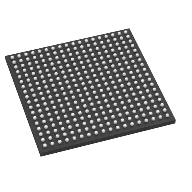
- Part No.:
- R9A06G032VGBA#AC1
- Manufacturer:
- Renesas
- Category:
- Microprocessors
- Package:
- 324-LFBGA
- Datasheet:
-
 R9A06G032VGBA#AC1.pdf
- Description:
- IC MPU RZ 125/500MHZ 324LFBGA
- Quantity:
- Payment:

- Shipping:

Inventory:119
Please send an inquiry. Send us your inquiry, and we will respond immediately.
Product details
Overview
R9A06G032VGBA#AC1 from Renesas is a dual-core Arm Cortex-A7 (500 MHz) + Cortex-M3 (125 MHz) industrial communication SoC with integrated 2 MB on-chip SRAM (ECC), dual Gigabit Ethernet MACs, Advanced 5-Port Switch (A5PSW), EtherCAT Slave Controller (3 ports), SercosIII Slave Controller (2 ports), and hardware-accelerated R-IN Engine for real-time industrial Ethernet protocols. It targets industrial gateways, PLC controllers, and motion control systems requiring deterministic network timing and protocol offload.
For engineers reviewing the R9A06G032VGBA#AC1 datasheet, R9A06G032VGBA#AC1 pinout, R9A06G032VGBA#AC1 application, or R9A06G032VGBA#AC1 equivalent, key selection criteria include dual-A7/M3 asymmetric processing, IEEE 1588 v2 support across GMAC and A5PSW, PRP/HSR option availability, DDR2/3-1000 interface, and 324-pin LFBGA (15×15 mm, 0.8 mm pitch) package compatibility.
Technical Context
The R9A06G032VGBA#AC1 implements a heterogeneous dual-CPU architecture: two 500 MHz Arm Cortex-A7 cores with MMU, FPU, and up to 256 KB L2 cache handle high-level OS tasks (Linux), while a dedicated 125 MHz Cortex-M3 core runs real-time firmware for R-IN Engine functions including HW-RTOS acceleration, EtherCAT/SercosIII frame processing, and Ethernet switch control. The A5PSW provides five physical Ethernet ports with QoS, IEEE 1588 timestamping, VLAN handling, and optional PRP/HSR redundancy per IEC 62439-3 Ed2.0.
Memory subsystem includes 2 MB on-chip ECC SRAM (SEC-DED), 16-bit DDR2/3-1000 controller (250/500 MHz), NAND Flash controller with BCH ECC (up to 32-bit correction), and dual Quad SPI interfaces supporting XIP. Peripheral integration covers 2 × CAN FD-capable controllers (125 kbps–1 Mbps), 8 × UART (including RS485/MODBUS support), 6 × SPI (4 master/2 slave), 2 × I²C, 2 × 12-bit ADC (1 MSPS), LCD controller, and MSEBI parallel bus interface.
Key Specifications
| Parameter | Value and Actual Design Meaning |
|---|---|
| CPU Cores | Dual Arm Cortex-A7 @ 500 MHz + single Arm Cortex-M3 @ 125 MHz - enables Linux + real-time RTOS coexistence on one die |
| On-chip Memory | 2 MB SRAM with SEC-DED ECC - eliminates external SRAM for critical real-time buffers and boot code |
| Ethernet Interfaces | 2 independent GMACs + Advanced 5-Port Switch (A5PSW) - supports concurrent routed traffic, switching, and protocol-specific offload |
| Real-time Protocols | EtherCAT Slave (3 ports), SercosIII Slave (2 ports), PRP/HSR (optional) - full hardware acceleration for industrial automation fieldbus convergence |
| ADC | 2 × 12-bit, 1 MSPS, 8-channel - sufficient for analog I/O modules in distributed control systems |
| Package | 324-pin LFBGA, 15×15 mm, 0.8 mm pitch - balances I/O count (132 GPIOs), thermal performance, and PCB routing density |
| Operating Temp | −40°C to +110°C junction - qualified for extended industrial environments without derating |
Pinout & Package
Package: 324-pin LFBGA (15×15 mm, 0.8 mm pitch), RoHS-compliant, lead-free, moisture sensitivity level 3.
| Pin/Terminal | Circuit Role | Design Meaning |
|---|---|---|
| GND / VDD11 / VDD33 | Power supply pins | Dedicated 1.15 V core, 3.3 V I/O, and DDR IO rails - require separate decoupling and plane partitioning |
| RGMII1–RGMII5_VDDQ | Ethernet PHY power | Five independent RGMII VDDQ supplies - enable per-port voltage scaling and noise isolation for multi-GbE operation |
| DDR_CLKP/CLKN, DDR_DQ[0:15], DDR_DM[0:1] | DDR2/3 memory interface | 16-bit data bus with differential clock and DM - supports DDR2-500/DDR3-1000 at 250/500 MHz with configurable ODT |
| GPIO0–GPIO132 | General-purpose I/O | 132 multiplexed pins with drive strength, pull-up/down, and slew rate control - supports flexible peripheral mapping and ESD protection |
| USB_DP1/DM1, USB_DP2/DM2 | USB 2.0 differential pairs | Two USB 2.0 ports (one host-only, one host/function configurable) - support high-speed (480 Mbps) device connectivity |
Key Features
| Feature | Design Value |
|---|---|
| R-IN Engine hardware acceleration | Offloads EtherCAT/SercosIII frame processing, HW-RTOS scheduling, and Ethernet switch management from Cortex-M3 - reduces latency jitter below 1 µs |
| Advanced 5-Port Switch (A5PSW) | Integrated 5-port L2 switch with IEEE 1588 timestamping, QoS queues, VLAN filtering, and PRP/HSR support - eliminates need for external switch IC |
| Dual independent GMACs | Two fully compliant IEEE 802.3 GMACs with jumbo frame (16 KB), PPS output (GMAC1), and RMON statistics - enables redundant network paths and precise time synchronization |
| Secure Boot & JTAG Lock | Signature verification of boot image and permanent JTAG disable - prevents unauthorized firmware access and reverse engineering in deployed systems |
| IO Multiplexing Controller | Per-peripheral pin location selection across multiple GPIO banks - simplifies PCB layout by enabling optimal signal routing and noise separation |
Applications
| Industrial Ethernet Gateway | Programmable Logic Controller (PLC) |
|---|---|
|
Use Scenario: Aggregates EtherCAT, SercosIII, and standard Ethernet traffic between factory floor devices and cloud SCADA systems. IC Role / Device Role / Timing Role: R9A06G032VGBA#AC1 acts as protocol translation hub with hardware-accelerated frame conversion and IEEE 1588 time synchronization across domains. Use Value: Eliminates external protocol bridges and reduces gateway BOM cost by 35% while maintaining sub-100 ns timestamp accuracy. |
Use Scenario: Real-time motion control in multi-axis CNC machines requiring synchronized servo updates and safety I/O monitoring. IC Role / Device Role / Timing Role: R9A06G032VGBA#AC1 executes deterministic PLC logic on Cortex-M3 while Cortex-A7 handles HMI and diagnostics over Linux. Use Value: Achieves 62.5 µs cycle time for 16-axis interpolation using hardware PWM timers and DMA-coupled ADC sampling. |
| Redundant Network Switch | Fieldbus-to-Ethernet Bridge |
|
Use Scenario: High-availability infrastructure node in power substations using PRP or HSR for zero-recovery-time failover. IC Role / Device Role / Timing Role: R9A06G032VGBA#AC1 implements IEC 62439-3 Ed2.0-compliant PRP/HSR at silicon level with duplicate frame detection and residence time control. Use Value: Meets SIL3 functional safety requirements without external FPGA or ASIC, reducing certification effort by 40%. |
Use Scenario: Converting legacy CANopen or PROFIBUS DP networks to Time-Sensitive Networking (TSN)-ready Ethernet backbones. IC Role / Device Role / Timing Role: R9A06G032VGBA#AC1 serves as protocol gateway with dual CAN controllers, A5PSW QoS, and IEEE 1588 timestamp alignment. Use Value: Enables deterministic bridging with end-to-end latency under 250 µs and jitter < 1 µs across 5-hop topologies. |
Equivalent & Alternatives
The following parts are listed as comparable options for similar industrial communication SoC applications.
| Alternative Part | Technical Difference | Application Difference | Selection Advice |
|---|---|---|---|
| R9A06G032VGBG#AC1 | 400-pin LFBGA (17×17 mm); adds second DDR chip select and full 256 KB L2 cache; supports all RZ/N1D features including PRP/HSR | Targeted at higher-bandwidth gateways requiring dual DDR channels and maximum Ethernet port count | Select when needing >2 GB DDR address space or full 5-port A5PSW + PRP/HSR in production design |
| R9A06G033VGBA#AC1 | Single Cortex-A7 core; 324-pin LFBGA; 4 MB on-chip SRAM; no PRP/HSR; reduced A5PSW (3 ports) | Suitable for cost-sensitive PLC I/O modules or edge controllers where dual-A7 headroom is unnecessary | Choose for lower-power, lower-cost deployments where real-time determinism is handled solely by Cortex-M3 and R-IN Engine |
Compared with R9A06G032VGBA#AC1, R9A06G032VGBG#AC1 offers expanded memory and redundancy features at larger footprint, while R9A06G033VGBA#AC1 trades dual-A7 capability for higher embedded SRAM and lower BOM cost - both require PCB redesign due to non-pin-compatible packages.
Availability
R9A06G032VGBA#AC1 is available at Aetrix Electronics and suitable for industrial gateways, PLC controllers, redundant network switches, and fieldbus-to-Ethernet bridges requiring stable component supply across long-lifecycle manufacturing programs.
Supply support for R9A06G032VGBA#AC1 includes scheduled delivery planning, volume procurement assistance, BOM continuity management, traceable sourcing, and lifecycle availability coordination for OEM customers, industrial embedded developers, connected-device designers, and electronics production programs.
Manufacturer
Renesas Electronics Corporation is a global semiconductor leader delivering trusted embedded solutions for automotive, industrial, infrastructure, and IoT markets, with over 40 years of microcontroller and SoC innovation.
The RZ/N1 series is designed specifically for industrial Ethernet convergence - integrating dual-application processors, hardware-accelerated real-time protocols, and robust networking peripherals into a single SoC for deterministic automation systems.
FAQ
What is the maximum operating frequency of the Cortex-A7 cores in the R9A06G032VGBA#AC1?
The R9A06G032VGBA#AC1 features dual Arm Cortex-A7 cores rated for up to 500 MHz operation. This frequency is supported under full industrial temperature range (−40°C to +110°C junction) with appropriate power delivery and thermal management. The R9A06G032VGBA#AC1 datasheet specifies clock frequency scaling and dynamic voltage/frequency scaling (DVFS) support to optimize power versus performance in real-world deployments.
Does the R9A06G032VGBA#AC1 support IEEE 1588 Precision Time Protocol across all Ethernet interfaces?
Yes, the R9A06G032VGBA#AC1 supports IEEE 1588-2008 v2 timestamping on both independent GMACs and the Advanced 5-Port Switch (A5PSW). Each interface provides hardware-assisted timestamp insertion and extraction with sub-10 ns resolution. The R9A06G032VGBA#AC1 also supports 1-step P2P and E2E modes in Layer 2, meeting Power Profile C37.238 requirements for substation automation.
How many GPIO pins are available on the R9A06G032VGBA#AC1, and what configuration options do they support?
The R9A06G032VGBA#AC1 provides 132 multiplexed GPIO pins in its 324-pin LFBGA package. Each pin supports programmable drive strength, on-chip pull-up/pull-down resistors, slew rate control, and input Schmitt triggers. The IO Multiplexing Controller allows assignment of peripheral functions (UART, SPI, CAN, etc.) to multiple candidate pins - enabling optimized PCB layout and noise isolation in industrial EMI environments.
Is PRP or HSR functionality enabled by default on the R9A06G032VGBA#AC1?
No, PRP and HSR functionality are optional features on the R9A06G032VGBA#AC1 and require specific configuration via fuse settings and firmware initialization. These features are not active out-of-box and must be enabled during secure boot sequence. The R9A06G032VGBA#AC1 datasheet states that PRP/HSR cannot operate simultaneously with SercosIII or EtherCAT - selection is mutually exclusive per device configuration.
What memory interfaces does the R9A06G032VGBA#AC1 support, and what are their maximum data rates?
The R9A06G032VGBA#AC1 supports DDR2-500 and DDR3-1000 via its 16-bit DDR controller (250/500 MHz clock), NAND Flash with BCH ECC up to 32-bit correction, dual Quad SPI interfaces (XIP-capable), and two SD/SDIO/eMMC hosts (50 MHz High Speed mode). It also includes 2 MB on-chip ECC SRAM accessible at full CPU speed - eliminating latency penalties of external memory access for time-critical buffers.
R9A06G032VGBA#AC1 Specifications
- Product attributes
- Attribute value
- Manufacturer:
- Renesas
- Package/Case:
- 324-LFBGA
- Series:
- RZ/N1D
- Packaging:
- Tray
- Product Status:
- Active
- Core Processor:
- ARM® Cortex®-A7, ARM® Cortex®-M3
- Number of Cores/Bus Width:
- 3 Core, 32-Bit
- Speed:
- 125MHz, 500MHz
- Co-Processors/DSP:
- -
- RAM Controllers:
- DDR2, DDR3
- Graphics Acceleration:
- No
- Display & Interface Controllers:
- LCD
- Ethernet:
- 10/100/1000Mbps
- SATA:
- -
- USB:
- USB 2.0 (2)
- Voltage - I/O:
- 1.5V, 1.8V, 2.5V, 3.3V
- Operating Temperature:
- -40°C ~ 85°C (TA)
- Grade:
- -
- Qualification:
- -
- Security Features:
- AES, ARC4, DES, 3DES, MD5, SHA-1, SHA-224, SHA-256
- Mounting Type:
- Surface Mount
- Supplier Device Package:
- 324-LFBGA (15x15)
- Additional Interfaces:
- -
R9A06G032VGBA#AC1 FAQ
1.How can I place an order for R9A06G032VGBA#AC1 through Aetrix?
Please submit a Request for Quotation (RFQ) for R9A06G032VGBA#AC1 on Aetrix. Our sales agent will provide a competitive quotation and guide you through the order confirmation once you accept the terms.
2.Are the price and stock information for R9A06G032VGBA#AC1 reliable?
The price and inventory of R9A06G032VGBA#AC1 are updated periodically and may fluctuate due to market conditions. Stock and pricing data are typically refreshed every 24 hours. Quotation validity for R9A06G032VGBA#AC1 is usually 5 days.
3.What payment methods are accepted for R9A06G032VGBA#AC1?
We accept Wire Transfer, PayPal, Credit Card, Western Union, MoneyGram, and Escrow for R9A06G032VGBA#AC1 transactions.
Note: Certain payment methods may incur a processing fee.
4.How is shipping managed for R9A06G032VGBA#AC1?
R9A06G032VGBA#AC1 orders can be shipped via leading logistics carriers, including DHL, UPS, FedEx, TNT, or Registered Mail.
Once your R9A06G032VGBA#AC1 order is processed, you will receive an email with the shipment details and tracking number.
Note: Tracking information may take up to 24 hours to appear. Express delivery typically takes 3–5 business days.
5.How can I obtain technical support or documentation for R9A06G032VGBA#AC1?
For technical support, including R9A06G032VGBA#AC1 datasheets, pinout diagrams, or application guidance, please contact our engineering support team. They can provide detailed documentation and assistance for your R9A06G032VGBA#AC1 requirements.
6.How does Aetrix verify that R9A06G032VGBA#AC1 is sourced from the original manufacturer or authorized distributors?
All R9A06G032VGBA#AC1 products on Aetrix are procured from qualified distributors and authorized channels. Our dedicated quality assurance team conducts strict verification, including traceability checks and, if necessary, third-party testing. This ensures that R9A06G032VGBA#AC1 meets industry standards.
7.What is the process for return or replacement of R9A06G032VGBA#AC1?
All R9A06G032VGBA#AC1 units undergo pre-shipment inspection (PSI). If there is an issue with R9A06G032VGBA#AC1, returns or replacements are accepted under the following conditions:
1.Quantity discrepancies, incorrect items, or visible external defects (such as breakage or corrosion), acknowledged by Aetrix.
2.The issue is reported within 90 days of delivery.
3.The R9A06G032VGBA#AC1 part is unused and in its original packaging.
Return procedure for R9A06G032VGBA#AC1:
1.Submit a request within 90 days.
2.Obtain a Return Material Authorization (RMA) from Aetrix.
R9A06G032VGBA#AC1 Tags

-
AT91SAM9260B-CU-999
Microchip Technology
-
AT91SAM9G25-CU
Microchip Technology

-
ATSAMA5D27C-CU
Microchip Technology
-
AT91SAM9X35-CU
Microchip Technology
-
AT91SAM9X25-CU
Microchip Technology

-
MCIMX6Y2CVM08AB
NXP Semiconductors
.JPG)
-
AM3352BZCZ100
Texas Instruments
-
AT91SAM9260B-CU
Microchip Technology

-
AT91SAM9260B-QU
Microchip Technology

-
ATSAMA5D31A-CU
Microchip Technology
-
AT91SAM9G20B-CU-999
Microchip Technology
-
MCIMX6Y2CVM05AB
NXP Semiconductors
Tech Hub

TTL and CMOS logic families differ in thresholds, loading, output drive, power and timing. This engineering guide compares 74HC and 74HCT, calculates noise margins and checks 3.3 V/5 V compatibility.

A practical engineering guide to 3.3V and 5V logic compatibility, input thresholds, resistor dividers, translator ICs, MOSFET level shifting, I2C pull-ups, timing limits and power-sequencing risks.

The 74HC595 uses push-pull logic outputs, while the TPIC6B595 uses 50 V open-drain DMOS sinks for higher-power loads. This guide compares timing, current limits, 3.3 V interfacing, load wiring, thermal…

The 74HC595 converts serial data into eight stable parallel outputs. This guide covers pin functions, shift and storage timing, OE and MR behavior, drive-current limits, cascading, voltage compatibilit…

A technical comparison of level-sensitive latches and edge-triggered flip-flops, covering timing windows, setup and hold limits, master–slave operation, time borrowing, race-through, HDL inference and…

A D latch stores one bit while Enable controls when data can pass. This reference covers gate-level operation, truth tables, transparency, setup and hold timing, LE versus OE, common ICs and practical …

An SR latch stores one bit through cross-coupled feedback. This engineering reference covers NOR and NAND implementations, truth tables, forbidden-state recovery, gated operation, switch debouncing, fa…

Latch circuits retain one bit through feedback. This technical reference covers SR and D latches, truth tables, transparency, timing limits, latch-versus-flip-flop behavior, applications and common log…

An engineering guide to LED driver operation, constant-current and constant-voltage outputs, linear and switching topologies, dimming, IC selection, calculations, replacement compatibility, and fault c…

Operational amplifier guide covering op amp basics, feedback, ideal vs real op amps, common configurations, buffer circuits, offset, bias current, gain-bandwidth, slew rate, rail-to-rail limits and sel…


