
 My Inquiry
 My Account


Renesas R9A07G075M24GBG#AC0
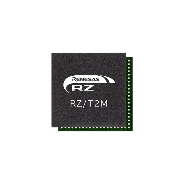
- Part No.:
- R9A07G075M24GBG#AC0
- Manufacturer:
- Renesas
- Category:
- Microprocessors
- Package:
- 320-LFBGA
- Datasheet:
-
 R9A07G075M24GBG#AC0.pdf
- Description:
- IC MPU 600MHZ/800MHZ 320LFBGA
- Quantity:
- Payment:

- Shipping:

Inventory:500
Please send an inquiry. Send us your inquiry, and we will respond immediately.
Product details
Overview
R9A07G075M24GBG#AC0 from Renesas Electronics is a dual-core Arm® Cortex®-R52 high-end real-time MPU targeting industrial motion control and EtherCAT slave applications. It operates at 200/400/800 MHz, integrates 2.0 MB on-chip SRAM with ECC, dual CAN-FD channels (ISO 11898-1), Ethernet MAC, and hardware accelerators for ΔΣ modulation and trigonometric functions - deployed in servo drives and PLCs requiring deterministic low-latency response.
For engineers reviewing the R9A07G075M24GBG#AC0 datasheet, R9A07G075M24GBG#AC0 pinout, R9A07G075M24GBG#AC0 application, or R9A07G075M24GBG#AC0 equivalent, key selection criteria include dual Cortex-R52 lock-step readiness (though DCLS not supported), CAN-FD data bit rate up to 8 Mbps, 2.0 MB ECC-protected SRAM, EtherCAT slave controller (3-port MII), and 320-pin FBGA package with 193 I/O pins.
Technical Context
The R9A07G075M24GBG#AC0 implements two Arm Cortex-R52 cores (r1p2) in asymmetric dual-core configuration: CPU0 includes 512 KB ATCM + 64 KB BTCM and full cache (16 KB I/D), while CPU1 provides 32 KB I/D cache only - no TCM. It uses Arm v8-R architecture with Little-endian data/instruction layout, Harvard pipeline, and dual-stage MPU (EL2/EL1) for safety-critical partitioning.
Real-time determinism is enforced via Event Link Controller (ELC) enabling module-triggered operation without CPU wake-up, MTU3/GPT timers with dead-time compensation and PWM synchronization, and isolated safety peripherals (4 GPT, 1 SCI, 1 IIC, CRC, RTC) mapped separately under EL2 protection. Security features include AES-128/192/256, ECDSA-P256, TRNG, and JTAG authentication - though security boot is disabled per part number suffix "M24".
Key Specifications
| Parameter | Value and Actual Design Meaning |
|---|---|
| CPU Core | Dual Arm Cortex-R52 (r1p2); CPU0 active with TCM/cache, CPU1 cache-only - enables asymmetric real-time + management partitioning. |
| Max Clock Frequency | 800 MHz (CPU), 200 MHz (system clock); supports deterministic timing-critical loop execution in motor control. |
| On-chip SRAM | 2.0 MB with SEC-DED ECC; eliminates external RAM dependency and reduces latency for servo trajectory buffers. |
| CAN-FD Interface | 2 channels, ISO 11898-1 compliant; nominal bit rate up to 1 Mbps, data bit rate up to 8 Mbps - suitable for high-bandwidth encoder feedback. |
| Ethernet Support | Ethernet MAC (1 port), EtherCAT slave controller (3 ports, MII), Ethernet switch (3 ports); enables multi-protocol industrial networking without external PHYs. |
| Package | 320-pin FBGA, 17 mm × 17 mm, 0.8 mm pitch; provides 193 configurable I/O pins with pin-mux flexibility for encoder, PWM, and analog interfaces. |
| Safety Features | Master MPU, CLMA clock monitor, CRC calculator (2 channels), DOC unit; supports IEC 61508 SIL3-ready system design. |
Pinout & Package
320-pin Fine-Pitch Ball Grid Array (FBGA), 17 mm × 17 mm, 0.8 mm pitch, RoHS-compliant, with exposed thermal pad. Pinout defined per R01DS0383EJ0130 Rev.1.30, Pages 42–122 (ball map A1–T20).
| Pin/Terminal | Circuit Role | Design Meaning |
|---|---|---|
| VDD (Balls A1–A4, C1–C4, etc.) | Core power supply | 1.1 V ±3% supply for Cortex-R52 cores and internal logic; requires low-noise regulation and local decoupling. |
| VCC18 (Balls D1–D4, F1–F4, etc.) | Analog & interface power | 1.8 V supply for USB PHY, ADC, TSU, PLL, and xSPI I/O; separate domain prevents noise coupling into precision analog paths. |
| VCC33 (Balls G1–G4, J1–J4, etc.) | I/O & USB power | 3.3 V supply for general-purpose I/O, RMII/MII, and USB transceiver; supports 3.3 V logic-level interfacing with industrial sensors and actuators. |
| CLKIN (Ball K1) | External clock input | 25 MHz crystal/resonator input for system clock generation; feeds PLL to derive CPU/system clocks with jitter tolerance per spec. |
| RES# (Ball L1) | Active-low reset input | Asynchronous hardware reset assertion; initiates full chip reset sequence including SRAM initialization and boot mode sampling. |
| MD[2:0] (Balls M1–O1) | Boot mode select | Configures boot source (xSPI0/1, bus, SCI, USB); determines initial code fetch path and memory mapping at power-on. |
Key Features
| Feature | Design Value |
|---|---|
| Dual Cortex-R52 with ECC-protected TCM | CPU0 includes 512 KB ATCM + 64 KB BTCM (0-wait ≤400 MHz), enabling ultra-low-latency real-time task execution without cache misses. |
| Integrated EtherCAT Slave Controller | Beckhoff-certified ESC IP core with 3-port MII interface; eliminates external ASIC/FPGA for EtherCAT slave implementation in drives. |
| Hardware ΔΣ Interface (DSMIF) | 2 units × 3 channels (6 total), supporting up to 6 external ΔΣ modulators; enables direct high-resolution current/voltage sensing in motor control. |
| Trigonometric Function Unit (TFU) | Simultaneous sine/cosine and arctangent/hypotk computation; accelerates field-oriented control (FOC) math without CPU load or floating-point library overhead. |
| Isolated Safety Peripherals | GPT (4 ch), SCI (1 ch), IIC (1 ch), SPI (1 ch), CRC (1 unit), RTC (1 unit) mapped under EL2 MPU - allows certified safe subsystem execution independent of main OS. |
Applications
| Servo Drive Control | Programmable Logic Controller (PLC) |
|---|---|
|
Use Scenario: High-precision closed-loop position/speed/torque control in industrial servo motors using EnDat/BiSS encoders and three-phase PWM inverters. IC Role / Device Role / Timing Role: Real-time motion controller executing FOC algorithms, generating synchronized 6-channel complementary PWM with dead-time compensation, and processing encoder feedback via hardware DSMIF and TFU. Use Value: 800 MHz dual-core execution + 2.0 MB on-chip SRAM eliminates external memory bottlenecks, enabling sub-10 µs current loop update times. |
Use Scenario: Deterministic I/O scanning, ladder logic execution, and fieldbus communication (EtherCAT/CAN-FD) in modular PLC backplanes. IC Role / Device Role / Timing Role: Central control processor managing cyclic process data exchange over EtherCAT slave interface, coordinating distributed I/O modules, and running safety-certified runtime firmware. Use Value: Dual Cortex-R52 with ELC-triggered peripheral operation ensures deterministic response to fieldbus events even during CPU standby - meeting IEC 61131-3 cycle time requirements. |
| Industrial Robotics Controller | Multi-Axis Motion System |
|
Use Scenario: Coordinated kinematic control across 6+ axes with real-time trajectory planning, collision avoidance, and safety monitoring. IC Role / Device Role / Timing Role: Main compute engine running RTOS-based motion planner, interfacing with absolute encoders via EnDat 2.2/BISS-C, and driving multi-channel PWM outputs with synchronized phase-shifted waveforms. Use Value: Hardware-accelerated TFU and MTU3/GPT timer cascade enable simultaneous inverse kinematics and precise PWM generation - reducing CPU utilization by >40% vs software-only implementation. |
Use Scenario: Synchronized motion control of conveyor belts, gantry systems, or CNC spindles requiring tight inter-axis coordination and jitter-free communication. IC Role / Device Role / Timing Role: Time-sensitive network node implementing IEEE 1588 PTP timestamping, EtherCAT distributed clocks, and deterministic CAN-FD messaging between master and slave axes. Use Value: Integrated GMAC + ETHSW + ESC provides full TSN-capable networking stack in one die - eliminating external switch ICs and reducing PCB layer count by 2–3 layers. |
Equivalent & Alternatives
The following parts are listed as comparable options for similar real-time industrial MPU applications.
| Alternative Part | Technical Difference | Application Difference | Selection Advice |
|---|---|---|---|
| R9A07G075M28GBG | Same package and dual-core configuration, but includes security boot, cryptographic accelerators, and JTAG authentication enabled. | Required for secure boot chain, firmware signing, and encrypted OTA updates in connected industrial devices. | Select R9A07G075M28GBG when end-product certification (e.g., IEC 62443) mandates hardware-rooted trust and secure firmware lifecycle management. |
| R9A07G075M26GBG | Identical package and memory, but supports Classical CAN (1 Mbps only) instead of CAN-FD; no security features enabled. | Suitable for legacy CAN-based I/O modules or cost-sensitive applications where 8 Mbps data burst is unnecessary. | Choose R9A07G075M26GBG if system uses only standard CAN networks and avoids CAN-FD bandwidth requirements - reduces BOM cost by ~$1.20/unit. |
Compared with R9A07G075M24GBG#AC0, R9A07G075M28GBG adds production-grade security features essential for cloud-connected edge devices, while R9A07G075M26GBG trades CAN-FD capability for lower cost in legacy-fieldbus deployments - all share identical real-time performance, EtherCAT, and motor-control acceleration.
Availability
R9A07G075M24GBG#AC0 is available at Aetrix Electronics and suitable for industrial servo drives, EtherCAT-enabled PLCs, and robotics controllers requiring stable component supply, long-term lifecycle support, and automotive-grade temperature resilience (−40°C to +125°C junction).
Supply support for R9A07G075M24GBG#AC0 includes scheduled delivery planning, volume procurement assistance, BOM continuity management, traceable sourcing, and lifecycle availability coordination for OEM customers, industrial embedded developers, connected-device designers, and electronics production programs.
Manufacturer
Renesas Electronics is a Japanese semiconductor manufacturer specializing in microcontrollers, MPUs, analog, and power solutions for industrial, automotive, and infrastructure markets - with leadership in real-time embedded processing.
The RZ/T2M group, including R9A07G075M24GBG#AC0, is designed specifically for deterministic industrial automation: integrating EtherCAT slave, CAN-FD, hardware motor control accelerators (TFU, DSMIF), and functional safety peripherals to replace FPGA+MPU combinations in servo and motion systems.
FAQ
Does R9A07G075M24GBG#AC0 support dual-core lock-step (DCLS) operation?
No, R9A07G075M24GBG#AC0 explicitly does not support Dual Core Lock Step (DCLS) per datasheet Section 1.1 Table 1.1. It implements asymmetric dual Cortex-R52 cores: CPU0 with full TCM and cache for real-time tasks, and CPU1 cache-only for background services. Safety-critical redundancy must be implemented via software partitioning and EL2 MPU isolation - not hardware lock-step.
What is the maximum CAN-FD data bit rate supported by R9A07G075M24GBG#AC0?
R9A07G075M24GBG#AC0 supports CAN-FD data bit rates up to 8 Mbps per channel, compliant with ISO 11898-1:2015. This is confirmed in Table 1.8 (CANFD module) and applies to both of its two CAN-FD channels - enabling high-bandwidth feedback from multi-turn absolute encoders or distributed I/O nodes in time-critical motion systems.
Is security functionality enabled on R9A07G075M24GBG#AC0?
No, security features including secure boot, cryptographic accelerators (AES/ECDSA/SHA), and JTAG authentication are disabled on R9A07G075M24GBG#AC0, as indicated by the "M24" suffix in the part number (per Table 1.16). For security-enabled variants, use R9A07G075M28GBG or R9A07G075M26GBG with appropriate boot configuration.
Which package and pin count does R9A07G075M24GBG#AC0 use?
R9A07G075M24GBG#AC0 uses a 320-pin Fine-Pitch Ball Grid Array (FBGA) package measuring 17 mm × 17 mm with 0.8 mm pitch and an exposed thermal pad. It provides 193 configurable I/O pins, as specified in Table 1.5 and Figure 1.1 of the R01DS0383EJ0130 datasheet - supporting dense peripheral routing for motor control and industrial networking.
Does R9A07G075M24GBG#AC0 include EtherCAT slave functionality?
Yes, R9A07G075M24GBG#AC0 integrates a Beckhoff-certified EtherCAT Slave Controller (ESC) with 3-port MII interface, as documented in Table 1.8 and Section 1.2. This enables direct implementation of EtherCAT slave nodes in servo drives and I/O terminals without external ASICs - supporting full EtherCAT protocol processing including distributed clocks and process data exchange.
R9A07G075M24GBG#AC0 Specifications
- Product attributes
- Attribute value
- Manufacturer:
- Renesas
- Package/Case:
- 320-LFBGA
- Series:
- -
- Packaging:
- Tray
- Product Status:
- Active
- Core Processor:
- ARM® Cortex®-R52
- Number of Cores/Bus Width:
- 2 Core, 32-Bit
- Speed:
- 600MHz, 800MHz
- Co-Processors/DSP:
- Multimedia; NEON™ SIMD
- RAM Controllers:
- -
- Graphics Acceleration:
- No
- Display & Interface Controllers:
- -
- Ethernet:
- 10/100/1000Mbps (2)
- SATA:
- -
- USB:
- USB 2.0 (2)
- Voltage - I/O:
- 1.8V, 3.3V
- Operating Temperature:
- -40°C ~ 125°C (TJ)
- Grade:
- -
- Qualification:
- -
- Security Features:
- -
- Mounting Type:
- Surface Mount
- Supplier Device Package:
- 320-LFBGA (17x17)
- Additional Interfaces:
- CANbus, I2C, SCI, SPI, WDT
R9A07G075M24GBG#AC0 FAQ
1.How can I place an order for R9A07G075M24GBG#AC0 through Aetrix?
Please submit a Request for Quotation (RFQ) for R9A07G075M24GBG#AC0 on Aetrix. Our sales agent will provide a competitive quotation and guide you through the order confirmation once you accept the terms.
2.Are the price and stock information for R9A07G075M24GBG#AC0 reliable?
The price and inventory of R9A07G075M24GBG#AC0 are updated periodically and may fluctuate due to market conditions. Stock and pricing data are typically refreshed every 24 hours. Quotation validity for R9A07G075M24GBG#AC0 is usually 5 days.
3.What payment methods are accepted for R9A07G075M24GBG#AC0?
We accept Wire Transfer, PayPal, Credit Card, Western Union, MoneyGram, and Escrow for R9A07G075M24GBG#AC0 transactions.
Note: Certain payment methods may incur a processing fee.
4.How is shipping managed for R9A07G075M24GBG#AC0?
R9A07G075M24GBG#AC0 orders can be shipped via leading logistics carriers, including DHL, UPS, FedEx, TNT, or Registered Mail.
Once your R9A07G075M24GBG#AC0 order is processed, you will receive an email with the shipment details and tracking number.
Note: Tracking information may take up to 24 hours to appear. Express delivery typically takes 3–5 business days.
5.How can I obtain technical support or documentation for R9A07G075M24GBG#AC0?
For technical support, including R9A07G075M24GBG#AC0 datasheets, pinout diagrams, or application guidance, please contact our engineering support team. They can provide detailed documentation and assistance for your R9A07G075M24GBG#AC0 requirements.
6.How does Aetrix verify that R9A07G075M24GBG#AC0 is sourced from the original manufacturer or authorized distributors?
All R9A07G075M24GBG#AC0 products on Aetrix are procured from qualified distributors and authorized channels. Our dedicated quality assurance team conducts strict verification, including traceability checks and, if necessary, third-party testing. This ensures that R9A07G075M24GBG#AC0 meets industry standards.
7.What is the process for return or replacement of R9A07G075M24GBG#AC0?
All R9A07G075M24GBG#AC0 units undergo pre-shipment inspection (PSI). If there is an issue with R9A07G075M24GBG#AC0, returns or replacements are accepted under the following conditions:
1.Quantity discrepancies, incorrect items, or visible external defects (such as breakage or corrosion), acknowledged by Aetrix.
2.The issue is reported within 90 days of delivery.
3.The R9A07G075M24GBG#AC0 part is unused and in its original packaging.
Return procedure for R9A07G075M24GBG#AC0:
1.Submit a request within 90 days.
2.Obtain a Return Material Authorization (RMA) from Aetrix.
R9A07G075M24GBG#AC0 Tags

-
AT91SAM9260B-CU-999
Microchip Technology
-
AT91SAM9G25-CU
Microchip Technology

-
ATSAMA5D27C-CU
Microchip Technology
-
AT91SAM9X35-CU
Microchip Technology
-
AT91SAM9X25-CU
Microchip Technology

-
MCIMX6Y2CVM08AB
NXP Semiconductors
.JPG)
-
AM3352BZCZ100
Texas Instruments
-
AT91SAM9260B-CU
Microchip Technology

-
AT91SAM9260B-QU
Microchip Technology

-
ATSAMA5D31A-CU
Microchip Technology
-
AT91SAM9G20B-CU-999
Microchip Technology
-
MCIMX6Y2CVM05AB
NXP Semiconductors
Tech Hub

TTL and CMOS logic families differ in thresholds, loading, output drive, power and timing. This engineering guide compares 74HC and 74HCT, calculates noise margins and checks 3.3 V/5 V compatibility.

A practical engineering guide to 3.3V and 5V logic compatibility, input thresholds, resistor dividers, translator ICs, MOSFET level shifting, I2C pull-ups, timing limits and power-sequencing risks.

The 74HC595 uses push-pull logic outputs, while the TPIC6B595 uses 50 V open-drain DMOS sinks for higher-power loads. This guide compares timing, current limits, 3.3 V interfacing, load wiring, thermal…

The 74HC595 converts serial data into eight stable parallel outputs. This guide covers pin functions, shift and storage timing, OE and MR behavior, drive-current limits, cascading, voltage compatibilit…

A technical comparison of level-sensitive latches and edge-triggered flip-flops, covering timing windows, setup and hold limits, master–slave operation, time borrowing, race-through, HDL inference and…

A D latch stores one bit while Enable controls when data can pass. This reference covers gate-level operation, truth tables, transparency, setup and hold timing, LE versus OE, common ICs and practical …

An SR latch stores one bit through cross-coupled feedback. This engineering reference covers NOR and NAND implementations, truth tables, forbidden-state recovery, gated operation, switch debouncing, fa…

Latch circuits retain one bit through feedback. This technical reference covers SR and D latches, truth tables, transparency, timing limits, latch-versus-flip-flop behavior, applications and common log…

An engineering guide to LED driver operation, constant-current and constant-voltage outputs, linear and switching topologies, dimming, IC selection, calculations, replacement compatibility, and fault c…

Operational amplifier guide covering op amp basics, feedback, ideal vs real op amps, common configurations, buffer circuits, offset, bias current, gain-bandwidth, slew rate, rail-to-rail limits and sel…


