
 My Inquiry
 My Account


Renesas RAA279971E3HNP#AA0
- Part No.:
- RAA279971E3HNP#AA0
- Manufacturer:
- Renesas
- Category:
- Encoders, Decoders, Converters
- Package:
- 32-VFQFN Exposed Pad
- Datasheet:
-
 RAA279971E3HNP#AA0.pdf
- Description:
- RAA279971 A5 AUTOMOTIVE HIGH DEF
- Quantity:
- Payment:

- Shipping:

Inventory:3,364
Please send an inquiry. Send us your inquiry, and we will respond immediately.
Product details
Overview
RAA279971E3HNP#AA0 from Renesas Electronics is a high-definition analog video encoder for automotive camera links, supporting 720p60 and 1080p30 input via MIPI-CSI2 (2-lane), DVP, or Pseudo BT.656, and encoding to CVBS using a built-in 10-bit DAC for transmission over coax/twisted pair up to 30 m. It integrates a PLL, test pattern generator, and independent Y/C amplitude control.
For engineers reviewing the RAA279971E3HNP#AA0 datasheet, RAA279971E3HNP#AA0 pinout, RAA279971E3HNP#AA0 application, or RAA279971E3HNP#AA0 equivalent, key selection criteria include AEC-Q100 qualification, MIPI/DVP interface coexistence, single-ended/differential CVBS output mode selection, 32-pin SQFN package, and 27 MHz crystal-based clocking architecture.
Technical Context
The RAA279971E3HNP#AA0 implements a dedicated analog video encoding pipeline with integrated PLL for pixel clock synthesis and supports simultaneous configuration of luminance and chrominance signal levels. Its MIPI-CSI2 1.1-compliant receiver operates in unidirectional mode with YUV422 format handling across two lanes.
Digital video input flexibility is achieved through shared DVP/MIPI pins and support for 8-/10-bit parallel interfaces-Pseudo BT.656 and DVP-with identical resolution support (720p30/60, 1080p30, e-mirror wide formats). Power management includes discrete Power Save and Power Down modes.
Key Specifications
| Parameter | Value and Actual Design Meaning |
|---|---|
| Video Input Interface | 2-lane MIPI-CSI2, DVP, or Pseudo BT.656 - enables pin-shared layout and multi-source camera compatibility |
| Max Input Resolution | 1080p30 or 720p60 - defines real-time HD capture capability for rear/surround-view systems |
| Analog Output Format | CVBS (single-ended, differential, pseudo-differential) - supports legacy display interfaces and noise-resilient cabling |
| DAC Resolution | 10-bit - provides 1024-level luminance/chrominance quantization for HD analog fidelity |
| Clock Source | Single 27 MHz crystal - eliminates external clock generators and reduces BOM count |
| I/O Voltage | Selectable 1.8 V or 3.3 V - allows interoperability with diverse SoC I/O domains |
| Qualification | AEC-Q100 Grade 2 - certified for under-hood automotive operation (-40°C to +105°C) |
Pinout & Package
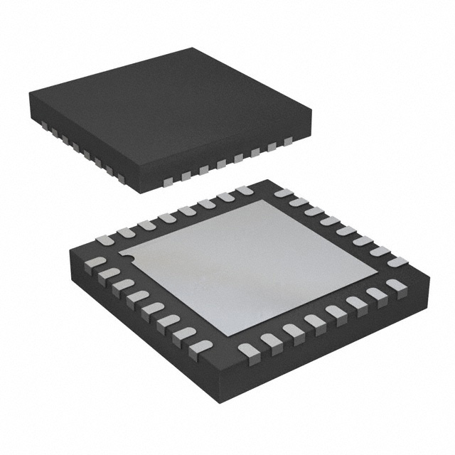
RAA279971E3HNP#AA0 is housed in a 32-lead SQFN package (5 mm × 5 mm, step-cut leads), optimized for automotive PCB space constraints and thermal performance.
| Pin/Terminal | Circuit Role | Design Meaning |
|---|---|---|
| CLKIN | Clock Input | Accepts 27 MHz fundamental-mode crystal connection for internal PLL reference |
| MIPI_D0P/DP0 | MIPI Data Lane 0+ / DVP Data Bit 0 | Shared pin for MIPI-CSI2 lane 0 positive or DVP parallel data bit 0 |
| MIPI_CLKP/DCLK | MIPI Clock+ / DVP Pixel Clock | Shared pin for MIPI clock differential pair or DVP pixel clock input |
| CVBS_OUT | Analog Video Output | Drives composite video signal in selectable single-ended or differential mode |
| I2C_SDA/I2S_SD | Two-Wire Interface Data | Bi-directional serial data line for register configuration and status readback |
| I2C_SCL/I2S_WS | Two-Wire Interface Clock | Serial clock input for I²C-compatible control of encoder registers |
Key Features
| Feature | Design Value |
|---|---|
| Software-selectable CVBS output mode | Enables system-level optimization: single-ended for cost-sensitive displays, differential for EMI-critical coax runs |
| Integrated test pattern generator | Eliminates external pattern sources during production test and field diagnostics |
| DVP/MIPI pin sharing | Reduces PCB layer count and routing complexity in multi-interface camera modules |
| Independent Y/C amplitude control | Allows fine-tuning of brightness and color saturation without altering source timing or format |
| Low-power operational modes | Power Save mode cuts dynamic power by >60%; Power Down halts all video processing for zero active current |
Applications
| Automotive Backup Camera Display | Automotive Surround View System |
|---|---|
Use Scenario: Real-time rear-view video feed displayed on center console or digital instrument cluster during reverse gear engagement. IC Role / Device Role / Timing Role: Analog video encoder converting camera sensor output to CVBS for legacy infotainment head units. Use Value: Enables plug-and-play integration with existing CVBS-capable displays while supporting 720p60 latency-critical imaging. | Use Scenario: Four-camera stitched bird's-eye view rendered on central display for low-speed maneuvering assistance. IC Role / Device Role / Timing Role: Synchronized HD video encoding node in multi-channel camera link subsystem. Use Value: Delivers time-aligned 1080p30 streams over coax with differential CVBS, reducing cable EMI in dense harness environments. |
| e-Mirror Camera Link | Automotive Digital Rearview Mirror |
Use Scenario: Wide-angle side camera replacing physical mirrors with electronic display in exterior mirror housings. IC Role / Device Role / Timing Role: High-bandwidth encoder supporting ultra-wide aspect ratio video (e.g., 1920×480) at 60 fps. Use Value: Maintains motion clarity and low latency using MIPI-CSI2 input and 27 MHz crystal-derived timing stability. | Use Scenario: Interior-mounted rear-facing camera feeding real-time video to electrochromic or LCD rearview mirror display. IC Role / Device Role / Timing Role: Low-power analog encoder operating in Power Save mode during vehicle idle to extend battery life. Use Value: Achieves <5 mW standby power while retaining fast wake-up (<100 µs) for immediate display activation. |
Equivalent & Alternatives
The following parts are listed as comparable options for similar analog video encoder applications.
| Alternative Part | Technical Difference | Application Difference | Selection Advice |
|---|---|---|---|
| MAX96705GTJ+T | 12-bit DAC, GMSL2 serial output (not CVBS), requires external serializer | Targets GMSL2-based camera links; no native coax CVBS output | Choose when migrating to serialized digital links and adding GMSL2 decoders |
| THS7353IPWPR | 3-channel SD/HD video amplifier (no encoding logic or MIPI input) | Requires upstream encoder IC; only drives CVBS output stage | Use only as output buffer stage downstream of a separate encoder like RAA279971E3HNP#AA0 |
Compared with MAX96705GTJ+T and THS7353IPWPR, the RAA279971E3HNP#AA0 uniquely integrates MIPI/DVP input decoding, 10-bit CVBS encoding, and AEC-Q100 qualification in one package-eliminating external DACs, serializers, or timing controllers required by alternatives.
Availability
RAA279971E3HNP#AA0 is available at Aetrix Electronics and suitable for automotive backup camera display, surround view system, and e-mirror camera link applications requiring stable component supply, AEC-Q100 compliance, and coaxial analog video transmission.
Supply support for RAA279971E3HNP#AA0 includes scheduled delivery planning, volume procurement assistance, BOM continuity management, traceable sourcing, and lifecycle availability coordination for OEM customers, industrial embedded developers, connected-device designers, and electronics production programs.
Manufacturer
Renesas Electronics Corporation is a global semiconductor manufacturer headquartered in Tokyo, Japan, specializing in microcontrollers, analog, power, and connectivity solutions for automotive, industrial, and IoT markets.
The RAA279971E3HNP#AA0 belongs to Renesas' Automotive Video Link family, designed specifically to replace legacy analog camera interfaces with robust, high-definition, AEC-Q100-qualified encoder/decoder pairs for safety-critical vision systems.
FAQ
What video interface standards does the RAA279971E3HNP#AA0 support?
The RAA279971E3HNP#AA0 supports MIPI-CSI2 1.1 (2-lane, YUV422), 8-/10-bit Digital Video Port (DVP), and 8-/10-bit Pseudo BT.656 parallel interfaces. It does not support HDMI, LVDS, or FPD-Link III. All three interfaces share physical pins to minimize footprint, and resolution support includes 720p30/60, 1080p30, and wide e-mirror formats. The RAA279971E3HNP#AA0 processes these inputs internally before encoding to analog CVBS.
Does the RAA279971E3HNP#AA0 require an external crystal oscillator?
No-the RAA279971E3HNP#AA0 uses a single 27 MHz fundamental-mode crystal connected to its CLKIN pin to generate all internal clocks via an integrated PLL. No external oscillator, clock buffer, or frequency synthesizer is needed. This simplifies design, reduces BOM cost, and improves timing stability. The RAA279971E3HNP#AA0 does not accept external clock signals; the crystal is mandatory for operation.
What CVBS output configurations does the RAA279971E3HNP#AA0 support?
The RAA279971E3HNP#AA0 supports three software-selectable CVBS output modes: single-ended, differential, and pseudo-differential. Single-ended drives standard 75 Ω coax to legacy displays; differential improves noise immunity over longer cables (up to 30 m); pseudo-differential enables compatibility with certain decoder inputs lacking true differential receivers. Mode selection is controlled via I²C register writes-no hardware changes are required. The RAA279971E3HNP#AA0 outputs only composite video (CVBS), not S-video or component.
Is the RAA279971E3HNP#AA0 qualified for automotive use?
Yes-the RAA279971E3HNP#AA0 is AEC-Q100 Grade 2 qualified, rated for operation from −40 °C to +105 °C ambient temperature, and manufactured in IATF 16949-certified facilities. It meets automotive reliability, ESD, and HTOL requirements. The device is intended for passenger vehicle camera systems-not safety-critical autonomous driving stacks-but is approved for backup, surround view, and e-mirror applications per ISO 26262 ASIL-B readiness documentation referenced in Renesas application notes. The RAA279971E3HNP#AA0 carries full automotive PPAP support.
Can the RAA279971E3HNP#AA0 generate test patterns without external video input?
Yes-the RAA279971E3HNP#AA0 includes an integrated test pattern generator that produces color bars, grayscale ramps, and crosshatch patterns directly from internal logic-no external video source or memory required. Patterns are configurable via I²C registers for resolution, format, and timing alignment. This feature enables factory calibration, cable integrity verification, and field diagnostics. The RAA279971E3HNP#AA0 outputs these patterns as valid CVBS signals identical to live video, making it usable for end-of-line testing and service mode validation.
RAA279971E3HNP#AA0 Specifications
- Product attributes
- Attribute value
- Manufacturer:
- Renesas
- Series:
- -
- Package/Case:
- 32-VFQFN Exposed Pad
- Packaging:
- Tray
- Product Status:
- Active
- Type:
- Encoder
- Applications:
- Camera
- Voltage - Supply, Analog:
- -
- Voltage - Supply, Digital:
- -
- Grade:
- -
- Qualification:
- -
- Mounting Type:
- Surface Mount, Wettable Flank
- Supplier Device Package:
- 32-SQFN (5x5)
RAA279971E3HNP#AA0 FAQ
1.How can I place an order for RAA279971E3HNP#AA0 through Aetrix?
Please submit a Request for Quotation (RFQ) for RAA279971E3HNP#AA0 on Aetrix. Our sales agent will provide a competitive quotation and guide you through the order confirmation once you accept the terms.
2.Are the price and stock information for RAA279971E3HNP#AA0 reliable?
The price and inventory of RAA279971E3HNP#AA0 are updated periodically and may fluctuate due to market conditions. Stock and pricing data are typically refreshed every 24 hours. Quotation validity for RAA279971E3HNP#AA0 is usually 5 days.
3.What payment methods are accepted for RAA279971E3HNP#AA0?
We accept Wire Transfer, PayPal, Credit Card, Western Union, MoneyGram, and Escrow for RAA279971E3HNP#AA0 transactions.
Note: Certain payment methods may incur a processing fee.
4.How is shipping managed for RAA279971E3HNP#AA0?
RAA279971E3HNP#AA0 orders can be shipped via leading logistics carriers, including DHL, UPS, FedEx, TNT, or Registered Mail.
Once your RAA279971E3HNP#AA0 order is processed, you will receive an email with the shipment details and tracking number.
Note: Tracking information may take up to 24 hours to appear. Express delivery typically takes 3–5 business days.
5.How can I obtain technical support or documentation for RAA279971E3HNP#AA0?
For technical support, including RAA279971E3HNP#AA0 datasheets, pinout diagrams, or application guidance, please contact our engineering support team. They can provide detailed documentation and assistance for your RAA279971E3HNP#AA0 requirements.
6.How does Aetrix verify that RAA279971E3HNP#AA0 is sourced from the original manufacturer or authorized distributors?
All RAA279971E3HNP#AA0 products on Aetrix are procured from qualified distributors and authorized channels. Our dedicated quality assurance team conducts strict verification, including traceability checks and, if necessary, third-party testing. This ensures that RAA279971E3HNP#AA0 meets industry standards.
7.What is the process for return or replacement of RAA279971E3HNP#AA0?
All RAA279971E3HNP#AA0 units undergo pre-shipment inspection (PSI). If there is an issue with RAA279971E3HNP#AA0, returns or replacements are accepted under the following conditions:
1.Quantity discrepancies, incorrect items, or visible external defects (such as breakage or corrosion), acknowledged by Aetrix.
2.The issue is reported within 90 days of delivery.
3.The RAA279971E3HNP#AA0 part is unused and in its original packaging.
Return procedure for RAA279971E3HNP#AA0:
1.Submit a request within 90 days.
2.Obtain a Return Material Authorization (RMA) from Aetrix.
RAA279971E3HNP#AA0 Tags

-
MCP2120T-I/SL
Microchip Technology

-
LICAL-ENC-MS001
TE Connectivity Linx
-
TW9990AT-NA1-GR
Renesas
-
TVP5151IPBSR
Texas Instruments
-
TVP5150AM1IPBSR
Texas Instruments
-
LICAL-DEC-MS001-T
TE Connectivity Linx
-
ADV7391BCPZ
Analog Devices Inc.
-
ADV7393BCPZ-REEL
Analog Devices Inc.
-
ADV7393BCPZ
Analog Devices Inc.
-
ADV7391WBCPZ
Analog Devices Inc.
-
ADV7181DBCPZ
Analog Devices Inc.

-
ADV7181CBSTZ-REEL
Analog Devices Inc.
Tech Hub

TTL and CMOS logic families differ in thresholds, loading, output drive, power and timing. This engineering guide compares 74HC and 74HCT, calculates noise margins and checks 3.3 V/5 V compatibility.

A practical engineering guide to 3.3V and 5V logic compatibility, input thresholds, resistor dividers, translator ICs, MOSFET level shifting, I2C pull-ups, timing limits and power-sequencing risks.

The 74HC595 uses push-pull logic outputs, while the TPIC6B595 uses 50 V open-drain DMOS sinks for higher-power loads. This guide compares timing, current limits, 3.3 V interfacing, load wiring, thermal…

The 74HC595 converts serial data into eight stable parallel outputs. This guide covers pin functions, shift and storage timing, OE and MR behavior, drive-current limits, cascading, voltage compatibilit…

A technical comparison of level-sensitive latches and edge-triggered flip-flops, covering timing windows, setup and hold limits, master–slave operation, time borrowing, race-through, HDL inference and…

A D latch stores one bit while Enable controls when data can pass. This reference covers gate-level operation, truth tables, transparency, setup and hold timing, LE versus OE, common ICs and practical …

An SR latch stores one bit through cross-coupled feedback. This engineering reference covers NOR and NAND implementations, truth tables, forbidden-state recovery, gated operation, switch debouncing, fa…

Latch circuits retain one bit through feedback. This technical reference covers SR and D latches, truth tables, transparency, timing limits, latch-versus-flip-flop behavior, applications and common log…

An engineering guide to LED driver operation, constant-current and constant-voltage outputs, linear and switching topologies, dimming, IC selection, calculations, replacement compatibility, and fault c…

Operational amplifier guide covering op amp basics, feedback, ideal vs real op amps, common configurations, buffer circuits, offset, bias current, gain-bandwidth, slew rate, rail-to-rail limits and sel…


