
 My Inquiry
 My Account


Microchip Technology RE46C100D8F

- Part No.:
- RE46C100D8F
- Manufacturer:
- Microchip Technology
- Category:
- Sensor and Detector Interfaces
- Package:
- 8-VFDFN Exposed Pad
- Datasheet:
-
 RE46C100D8F.pdf
- Description:
- IC HORN DRIVER 8DFN
- Quantity:
- Payment:

- Shipping:

Inventory:3,001
Please send an inquiry. Send us your inquiry, and we will respond immediately.
Product details
Overview
RE46C100D8F from Microchip Technology is a CMOS piezoelectric horn driver IC designed for self-oscillating and direct-drive alarm applications. It integrates feedback control, push-pull output stage, and horn enable logic, with <100 nA quiescent current, 20 Ω typical RON at 9 V, and operation from 6–16 V - enabling ultra-low-power battery-operated smoke and CO detectors.
For engineers reviewing the RE46C100D8F datasheet, RE46C100D8F pinout, RE46C100D8F application, or RE46C100D8F equivalent, key selection considerations include its dual-mode horn drive capability (self-oscillating via FEED pin or external signal input), HRNEN-active-high enable timing, and thermal performance in 2×3 mm DFN with exposed pad - critical for compact, long-life safety devices.
Technical Context
The RE46C100D8F implements a dedicated analog push-pull output stage driving HORNB and HORNS complementary outputs to excite piezoelectric transducers. Its internal feedback path accepts signals from the horn's feedback electrode via the FEED pin, enabling self-oscillation without external oscillator components.
Logic-level HRNEN control (VIL ≤ 1 V, VIH ≥ 2.3 V) directly gates the output stage, allowing PWM modulation of audible alerts. The device operates across –40°C to +85°C and supports wide supply range (6–16 V), with FEED pin rated to –10 V to +22 V for robust feedback interface handling.
Key Specifications
| Parameter | Value and Actual Design Meaning |
|---|---|
| Supply Voltage Range | 6 V to 16 V - supports single 9 V battery operation with margin for aging and cold-temperature drop |
| Quiescent Current | <100 nA - enables >10-year battery life in smoke detector standby mode |
| Output RON | 20 Ω typical at 9 V - ensures efficient power transfer to piezo load with minimal heat generation |
| HORN Enable Threshold | VIH ≥ 2.3 V, VIL ≤ 1 V - compatible with standard CMOS/LVTTL logic without level-shifting |
| FEED Pin Voltage Range | –10 V to +22 V - accommodates high-swing feedback signals from piezoelectric elements |
| Operating Temperature | –40°C to +85°C - qualified for residential and commercial indoor safety equipment environments |
| Thermal Resistance (θJA) | 75°C/W (DFN package) - enables reliable operation in sealed enclosures with limited airflow |
Pinout & Package
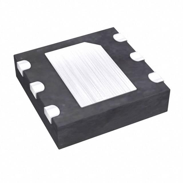
RE46C100D8F uses an 8-lead 2×3 mm DFN package with exposed thermal pad (EP), optimized for low-profile, high-reliability alarm modules. The EP must be soldered to VSS for thermal and electrical integrity.
| Pin/Terminal | Circuit Role | Design Meaning |
|---|---|---|
| 1, 3 | NC | No connection - left unconnected per design; no internal circuitry attached |
| 2 | VDD | Main positive supply input - connects to battery or regulated 6–16 V rail |
| 4 | FEED | Feedback/signal input - receives oscillation feedback from piezo horn or external drive signal |
| 5 | VSS | Ground reference - ties to system common and exposed thermal pad (EP) |
| 6 | HORNB | Output A - drives metal electrode of piezoelectric transducer |
| 7 | HORNS | Output B - complementary output driving ceramic electrode for push-pull excitation |
| 8 | HRNEN | Enable control - logic high activates output stage; logic low silences horn |
| 9 (EP) | Exposed Pad | Thermal & electrical ground - must be soldered to PCB VSS plane for thermal dissipation and noise reduction |
Key Features
| Feature | Design Value |
|---|---|
| Ultra-low standby current | <100 nA enables multi-year battery life in always-on smoke/CO detectors |
| Integrated self-oscillation feedback path | Eliminates need for external oscillator or timing components in piezo horn circuits |
| Complementary push-pull outputs | HORNB/HORNS deliver balanced drive to maximize sound pressure output from piezo elements |
| Wide-voltage FEED input tolerance | –10 V to +22 V rating prevents damage from piezo back-EMF transients |
| HRNEN modulated enable | Allows direct PWM control of audible alert tone without external gate drivers |
Applications
| Smoke Detectors | CO Detectors |
|---|---|
Use Scenario: Battery-powered residential smoke alarm requiring >10-year shelf life and loud audible alert on sensor trigger. IC Role / Device Role / Timing Role: Piezoelectric horn driver with integrated feedback control and low-IQ enable logic. Use Value: Enables self-oscillating horn operation using only one external resistor, reducing BOM count and PCB area while maintaining UL-listed sound output. |
Use Scenario: Portable CO monitor with intermittent sampling and periodic audible warning during alarm state. IC Role / Device Role / Timing Role: Low-power horn driver activated by microcontroller GPIO via HRNEN pin. Use Value: Sub-100 nA quiescent current preserves coin-cell or AAA battery life between CO events; FEED pin tolerance prevents latch-up from piezo ringing. |
| Personal Security Alarms | Electronic Toys |
Use Scenario: Handheld panic button emitting piercing 3–4 kHz tone when triggered. IC Role / Device Role / Timing Role: Direct-drive horn controller accepting external square-wave input via FEED pin. Use Value: Eliminates need for discrete MOSFETs or driver ICs; 20 Ω RON delivers full battery voltage swing to piezo for maximum SPL. |
Use Scenario: Low-cost educational toy with simple on/off sound effects powered by alkaline cells. IC Role / Device Role / Timing Role: Integrated horn driver with NC pins simplifying layout and reducing assembly cost. Use Value: DFN package enables compact PCB footprint; wide 6–16 V range tolerates fresh-to-dead battery voltage without regulation. |
Equivalent & Alternatives
The following parts are listed as comparable options for similar piezoelectric horn driver applications.
| Alternative Part | Technical Difference | Application Difference | Selection Advice |
|---|---|---|---|
| RE46C100E8F | Same die, PDIP-8 package (300 mil); θJA = 89.3°C/W; no exposed thermal pad | Better suited for through-hole prototyping or legacy wave-soldered assemblies | Select when manual assembly, socketing, or higher thermal margin at lower power density is required |
| RE46C100S8F | Same die, SOIC-8 package; θJA = 149.5°C/W; larger footprint than DFN | Preferred for reflow-compatible designs where DFN placement or inspection is constrained | Choose when existing SOIC land patterns exist or thermal load is light (<5 mA average output current) |
Compared with RE46C100E8F and RE46C100S8F, the RE46C100D8F offers the lowest thermal resistance (75°C/W) and smallest footprint - making it optimal for space-constrained, high-volume smoke detector modules where thermal management and PCB area are critical.
Availability
RE46C100D8F is available at Aetrix Electronics and suitable for smoke detectors, CO detectors, and personal security alarms requiring stable component supply, long-lifecycle support, and RoHS-compliant lead-free packaging.
Supply support for RE46C100D8F includes scheduled delivery planning, volume procurement assistance, BOM continuity management, traceable sourcing, and lifecycle availability coordination for OEM customers, industrial embedded developers, connected-device designers, and electronics production programs.
Manufacturer
Microchip Technology Inc. is a leading provider of microcontrollers, analog devices, and timing solutions, headquartered in Chandler, Arizona, with global design and manufacturing operations.
The RE46C100D8F belongs to Microchip's safety ASIC product line, engineered specifically for ultra-low-power, high-reliability audible alarm functions in life-safety equipment - emphasizing quiescent current minimization, piezo interface robustness, and qualification across extended temperature ranges.
FAQ
What is the function of the FEED pin on the RE46C100D8F?
The FEED pin on the RE46C100D8F serves a dual role: in self-oscillating mode, it connects to the feedback electrode of a three-terminal piezoelectric horn to sustain oscillation; in direct-drive mode, it accepts an external square-wave signal to drive two-terminal horns. Its –10 V to +22 V rating protects against piezo-induced voltage spikes, ensuring reliable operation without clamping diodes in the RE46C100D8F circuit.
Can the RE46C100D8F drive both two-terminal and three-terminal piezoelectric horns?
Yes, the RE46C100D8F supports both configurations. For three-terminal self-oscillating horns, the FEED pin is connected to the feedback electrode through a current-limiting resistor. For two-terminal horns, FEED acts as an external signal input, while HRNEN enables/disables the output stage. This flexibility allows a single RE46C100D8F design to serve multiple horn types without hardware changes.
What is the purpose of the exposed thermal pad (EP) on the RE46C100D8F DFN package?
The exposed thermal pad (Pin 9, EP) on the RE46C100D8F DFN package provides a low-thermal-resistance path from the die to the PCB ground plane. It must be soldered to VSS for effective heat dissipation - reducing junction temperature by up to 30°C versus non-connected EP - and also improves electrical noise immunity. Microchip specifies EP connection as mandatory for reliable RE46C100D8F operation in continuous-tone applications.
How does the HRNEN pin control the output of the RE46C100D8F?
The HRNEN pin on the RE46C100D8F is an active-high enable input: logic high (≥2.3 V) activates the push-pull output stage on HORNB and HORNS, while logic low (≤1 V) disables output and places both pins in high-impedance state. This allows precise timing control - including PWM modulation of tone duration - and eliminates audible click noise during enable/disable transitions in the RE46C100D8F application.
Is the RE46C100D8F compatible with 3.3 V logic systems?
No, the RE46C100D8F is not directly compatible with 3.3 V logic. Its HRNEN input requires VIH ≥ 2.3 V minimum, but the device itself operates from 6–16 V supply and lacks internal level-shifting. Driving HRNEN from a 3.3 V MCU GPIO may result in marginal or unreliable enable behavior. A simple N-channel MOSFET level shifter or buffer is recommended to ensure robust RE46C100D8F activation in mixed-voltage systems.
RE46C100D8F Specifications
- Product attributes
- Attribute value
- Manufacturer:
- Microchip Technology
- Package/Case:
- 8-VFDFN Exposed Pad
- Series:
- -
- Packaging:
- Tube
- Product Status:
- Active
- Programmable:
- Not Verified
- Type:
- Controller
- Input Type:
- -
- Output Type:
- -
- Current - Supply:
- 100 nA
- Operating Temperature:
- -40°C ~ 85°C
- Grade:
- -
- Qualification:
- -
- Mounting Type:
- Surface Mount
- Supplier Device Package:
- 8-DFN (2x3)
RE46C100D8F FAQ
1.How can I place an order for RE46C100D8F through Aetrix?
Please submit a Request for Quotation (RFQ) for RE46C100D8F on Aetrix. Our sales agent will provide a competitive quotation and guide you through the order confirmation once you accept the terms.
2.Are the price and stock information for RE46C100D8F reliable?
The price and inventory of RE46C100D8F are updated periodically and may fluctuate due to market conditions. Stock and pricing data are typically refreshed every 24 hours. Quotation validity for RE46C100D8F is usually 5 days.
3.What payment methods are accepted for RE46C100D8F?
We accept Wire Transfer, PayPal, Credit Card, Western Union, MoneyGram, and Escrow for RE46C100D8F transactions.
Note: Certain payment methods may incur a processing fee.
4.How is shipping managed for RE46C100D8F?
RE46C100D8F orders can be shipped via leading logistics carriers, including DHL, UPS, FedEx, TNT, or Registered Mail.
Once your RE46C100D8F order is processed, you will receive an email with the shipment details and tracking number.
Note: Tracking information may take up to 24 hours to appear. Express delivery typically takes 3–5 business days.
5.How can I obtain technical support or documentation for RE46C100D8F?
For technical support, including RE46C100D8F datasheets, pinout diagrams, or application guidance, please contact our engineering support team. They can provide detailed documentation and assistance for your RE46C100D8F requirements.
6.How does Aetrix verify that RE46C100D8F is sourced from the original manufacturer or authorized distributors?
All RE46C100D8F products on Aetrix are procured from qualified distributors and authorized channels. Our dedicated quality assurance team conducts strict verification, including traceability checks and, if necessary, third-party testing. This ensures that RE46C100D8F meets industry standards.
7.What is the process for return or replacement of RE46C100D8F?
All RE46C100D8F units undergo pre-shipment inspection (PSI). If there is an issue with RE46C100D8F, returns or replacements are accepted under the following conditions:
1.Quantity discrepancies, incorrect items, or visible external defects (such as breakage or corrosion), acknowledged by Aetrix.
2.The issue is reported within 90 days of delivery.
3.The RE46C100D8F part is unused and in its original packaging.
Return procedure for RE46C100D8F:
1.Submit a request within 90 days.
2.Obtain a Return Material Authorization (RMA) from Aetrix.
RE46C100D8F Tags

-
RE46C100S8TF
Microchip Technology

-
XTR111AIDRCR
Texas Instruments

-
XTR111AIDGQR
Texas Instruments

-
XTR117AIDGKR
Texas Instruments
-
XTR111AIDGQT
Texas Instruments

-
XTR115UA/2K5
Texas Instruments
-
MAX14626ETT+T
Analog Devices Inc./Maxim Integrated
-
XTR116UA/2K5
Texas Instruments
-
XTR115U/2K5
Texas Instruments
-
XTR116U/2K5
Texas Instruments

-
PGA308AIDGSR
Texas Instruments
-
XTR300AIRGWR
Texas Instruments
Tech Hub

TTL and CMOS logic families differ in thresholds, loading, output drive, power and timing. This engineering guide compares 74HC and 74HCT, calculates noise margins and checks 3.3 V/5 V compatibility.

A practical engineering guide to 3.3V and 5V logic compatibility, input thresholds, resistor dividers, translator ICs, MOSFET level shifting, I2C pull-ups, timing limits and power-sequencing risks.

The 74HC595 uses push-pull logic outputs, while the TPIC6B595 uses 50 V open-drain DMOS sinks for higher-power loads. This guide compares timing, current limits, 3.3 V interfacing, load wiring, thermal…

The 74HC595 converts serial data into eight stable parallel outputs. This guide covers pin functions, shift and storage timing, OE and MR behavior, drive-current limits, cascading, voltage compatibilit…

A technical comparison of level-sensitive latches and edge-triggered flip-flops, covering timing windows, setup and hold limits, master–slave operation, time borrowing, race-through, HDL inference and…

A D latch stores one bit while Enable controls when data can pass. This reference covers gate-level operation, truth tables, transparency, setup and hold timing, LE versus OE, common ICs and practical …

An SR latch stores one bit through cross-coupled feedback. This engineering reference covers NOR and NAND implementations, truth tables, forbidden-state recovery, gated operation, switch debouncing, fa…

Latch circuits retain one bit through feedback. This technical reference covers SR and D latches, truth tables, transparency, timing limits, latch-versus-flip-flop behavior, applications and common log…

An engineering guide to LED driver operation, constant-current and constant-voltage outputs, linear and switching topologies, dimming, IC selection, calculations, replacement compatibility, and fault c…

Operational amplifier guide covering op amp basics, feedback, ideal vs real op amps, common configurations, buffer circuits, offset, bias current, gain-bandwidth, slew rate, rail-to-rail limits and sel…


