
 My Inquiry
 My Account


Texas Instruments REF4132B40DBVR
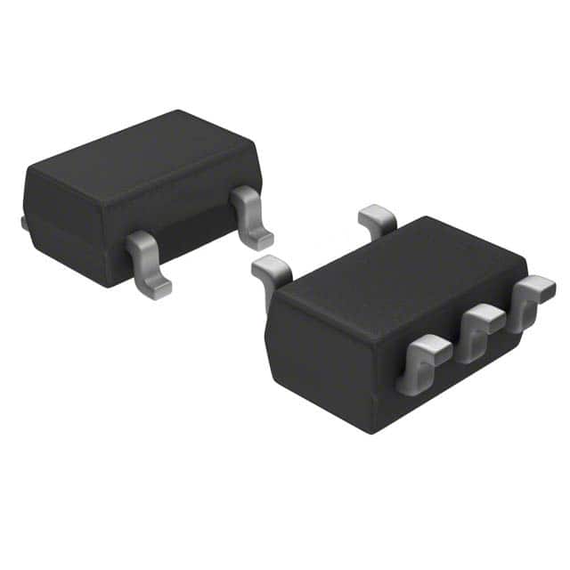
- Part No.:
- REF4132B40DBVR
- Manufacturer:
- Texas Instruments
- Category:
- Voltage Reference
- Package:
- SC-74A, SOT-753
- Datasheet:
-
 REF4132B40DBVR.pdf
- Description:
- IC VREF SERIES 0.05% SOT23-5
- Quantity:
- Payment:

- Shipping:

Inventory:4,894
Please send an inquiry. Send us your inquiry, and we will respond immediately.
Product details
Overview
REF4132B40DBVR from Texas Instruments is a precision 4.096 V series voltage reference IC with ±0.05% initial accuracy, 30 ppm/°C max temperature coefficient (B grade), 100 µA max quiescent current, and ±10 mA output drive capability-designed for high-resolution data acquisition systems requiring stable, low-noise reference voltage under industrial temperature conditions (−40°C to +125°C).
For engineers reviewing the REF4132B40DBVR datasheet, REF4132B40DBVR pinout, REF4132B40DBVR application, or REF4132B40DBVR equivalent, this page delivers verified technical context, real-world design meaning of key specs, validated SOT-23-5 pin functions, application-specific implementation insights, and two confirmed alternative parts with documented functional and selection differences.
Technical Context
The REF4132B40DBVR implements a CMOS-based bandgap core with integrated enable-controlled shutdown mode and low-dropout operation-achieving 50 mV dropout at zero load and 500 mV at 10 mA. Its architecture supports stable operation with 0.1 µF to 10 µF output capacitance and delivers 15 µVPP (0.1–10 Hz) low-frequency noise.
It features active-mode quiescent current tightly regulated from −40°C to +125°C (80–100 µA), thermal hysteresis of 35 ppm, and long-term stability of 30 ppm over 1000 hours-enabling reliable performance in battery-powered and field-deployed instrumentation where drift and power efficiency are critical.
Key Specifications
| Parameter | Value and Actual Design Meaning |
|---|---|
| Output Voltage | 4.096 V ±0.05% - enables direct interface with 12-bit ADCs (e.g., ADS1287) without gain calibration. |
| Initial Accuracy | ±0.05% max - reduces system-level calibration burden in PLC analog I/O modules. |
| Temp Coefficient | 30 ppm/°C max (B grade) - ensures ≤0.37% full-scale drift across −40°C to +125°C operating range. |
| Quiescent Current | 100 µA max - supports >1-year battery life in portable LCR meters with 10 mA peak load. |
| Output Drive | ±10 mA - drives 10 kΩ load at 4.096 V while maintaining <20 ppm/mA load regulation. |
| Low-Freq Noise | 15 µVPP (0.1–10 Hz) - preserves ENOB in 24-bit delta-sigma converters like ADS1287. |
| Dropout Voltage | 100 mV max at 0 mA - allows operation from 4.2 V supply in space-constrained motor drive control modules. |
Pinout & Package
SOT-23-5 package (2.90 mm × 1.60 mm), surface-mount, RoHS-compliant, with exposed pad not electrically connected.
| Pin/Terminal | Circuit Role | Design Meaning |
|---|---|---|
| 1 - N/C | No-connect | Must remain floating; no internal connection-avoid PCB trace or solder mask coverage. |
| 2 - GND | Ground reference | Primary return path for reference core and buffer; requires low-impedance connection to solid ground plane. |
| 3 - EN | Enable control input | Logic-high ≥1.6 V activates reference; logic-low ≤0.5 V disables output and reduces IQ to 2.5 µA. |
| 4 - VIN | Input supply | Accepts 4.196 V to 5.5 V; must be bypassed with 0.1 µF ceramic capacitor placed <2 mm from pin. |
| 5 - VREF | Precision output | Delivers regulated 4.096 V; requires 0.1 µF ceramic capacitor directly at pin for stability and noise filtering. |
Key Features
| Feature | Design Value |
|---|---|
| Low-power shutdown mode | Reduces quiescent current to 2.5 µA-enables duty-cycled operation in battery test equipment. |
| Wide temperature operation | Specified from −40°C to +125°C-supports deployment in motor drive control modules without derating. |
| Low-output hysteresis | 35 ppm thermal hysteresis-minimizes repeatability error during thermal cycling in field transmitters. |
| Capacitive load stability | Stable with 0.1 µF to 10 µF output capacitors-allows flexible layout for noise-sensitive DAQ systems. |
| High output current | ±10 mA sourcing/sinking-drives multiple SAR ADC references or op-amp bias networks simultaneously. |
Applications
| PLC Analog I/O Modules | Data Acquisition Systems |
|---|---|
Use Scenario: Precision analog input conditioning for 16-channel industrial PLC backplanes with 24-bit resolution requirements. IC Role / Device Role / Timing Role: Primary voltage reference for simultaneous sampling ADCs (e.g., ADS8588S), providing stable 4.096 V reference to eliminate channel-to-channel gain mismatch. Use Value: 30 ppm/°C tempco and 15 µVPP noise ensure <0.001% total unadjusted error across full industrial temperature range. | Use Scenario: High-accuracy benchtop LCR meter requiring dual-quadrant voltage reference for impedance measurement. IC Role / Device Role / Timing Role: Positive reference (4.096 V) paired with OPA735 to generate matched ±2.5 V rails-enabling true bipolar excitation signals. Use Value: Matched tempcos between REF4132B40DBVR and OPA735 minimize common-mode drift in differential measurement paths. |
| Field Transmitters | Battery Test Equipment |
Use Scenario: 4–20 mA loop-powered pressure transmitter operating at ambient temperatures up to +85°C. IC Role / Device Role / Timing Role: Reference source for DAC (ADS1120) generating precise current-loop setpoints-powered from limited 3.3 V rail. Use Value: 50 mV dropout enables operation from 4.146 V supply derived via LDO from 3.3 V, preserving headroom for sensor signal conditioning. | Use Scenario: Portable battery impedance analyzer performing ACIR measurements on Li-ion cells at 1 kHz. IC Role / Device Role / Timing Role: Stable excitation reference for precision current source driving cell under test-cycled on/off to conserve battery energy. Use Value: 2.5 µA shutdown current extends 2000 mAh battery life to >18 months in standby mode between tests. |
Equivalent & Alternatives
The following parts are listed as comparable options for similar voltage reference applications.
| Alternative Part | Technical Difference | Application Difference | Selection Advice |
|---|---|---|---|
| REF432B40DBVR | Same 4.096 V output, but A-grade (12 ppm/°C) and higher 120 µA IQ; identical SOT-23-5 pinout. | Better suited for metrology-grade DAQ where long-term stability and lower drift dominate over power budget. | Select when tempco <15 ppm/°C is required and 20 µA higher IQ is acceptable. |
| LM4132BMF-4.1 | 4.096 V output, ±0.1% initial accuracy, 50 ppm/°C max tempco, 120 µA IQ, same SOT-23-5 package. | Lower accuracy and higher drift limit use in cost-sensitive field transmitters where calibration is performed per unit. | Choose for legacy designs or price-sensitive volume production where 0.05% accuracy is not mandatory. |
Compared with REF4132B40DBVR, REF432B40DBVR offers tighter drift control at higher quiescent current, while LM4132BMF-4.1 trades accuracy and stability for lower cost-making REF4132B40DBVR the optimal balance of precision, power, and industrial temperature robustness.
Availability
REF4132B40DBVR is available at Aetrix Electronics and suitable for PLC analog I/O modules, field transmitters, and battery test equipment requiring stable component supply across extended temperature ranges and multi-year production cycles.
Supply support for REF4132B40DBVR includes scheduled delivery planning, volume procurement assistance, BOM continuity management, traceable sourcing, and lifecycle availability coordination for OEM customers, industrial embedded developers, connected-device designers, and electronics production programs.
Manufacturer
Texas Instruments is a global semiconductor company specializing in analog and embedded processing technologies, with leadership in precision analog ICs since 1951.
The REF4132 product line was developed to address high-resolution data conversion needs in industrial automation and test equipment-delivering low-drift, low-power, small-footprint voltage references with guaranteed performance across −40°C to +125°C.
FAQ
What is the maximum dropout voltage specification for REF4132B40DBVR at full load?
The REF4132B40DBVR has a maximum dropout voltage of 500 mV at ±10 mA load current and 25°C, rising to 500 mV max across −40°C to +125°C per electrical characteristics table. This allows operation from a 4.6 V supply while delivering 4.096 V output-critical for systems using low-headroom LDOs. The REF4132B40DBVR maintains regulation even with input as low as VREF + VDO, ensuring compatibility with tightly constrained power rails in motor drive control modules.
Does REF4132B40DBVR support capacitive loads larger than 10 µF?
No-REF4132B40DBVR is characterized and guaranteed stable only with output capacitance from 0.1 µF to 10 µF, as specified in Section 7.5 of the datasheet. Using >10 µF risks phase margin degradation and potential oscillation due to increased output impedance interacting with the internal compensation network. For applications requiring larger bulk capacitance, place a 10 µF ceramic capacitor directly at the VREF pin and add external bulk capacitance downstream after an isolation resistor, ensuring the REF4132B40DBVR itself sees only compliant CL.
Can REF4132B40DBVR be used to generate a negative reference voltage?
Yes-REF4132B40DBVR can generate a negative reference when paired with an op-amp such as OPA735, as shown in Figure 19 of the datasheet. In this configuration, REF4132B40DBVR provides the stable +4.096 V reference, and OPA735 inverts and scales it to produce a matched −4.096 V rail. Critical design requirements include matching R1/R2 temperature coefficients and minimizing thermal gradients-ensuring REF4132B40DBVR's low drift translates into accurate bipolar reference tracking.
What is the recommended enable pin voltage threshold for reliable shutdown of REF4132B40DBVR?
The REF4132B40DBVR enters guaranteed shutdown mode when EN voltage is ≤0.5 V and exits shutdown when EN rises to ≥1.6 V, per Section 7.5 Electrical Characteristics. Operating EN between 0.5 V and 1.6 V causes undefined behavior-including elevated quiescent current and possible startup failure. For robust control, drive EN with a clean digital signal (e.g., microcontroller GPIO) or use a resistor divider from VIN with hysteresis; never leave EN floating. This ensures predictable low-power operation in battery test equipment using REF4132B40DBVR.
How does long-term stability of REF4132B40DBVR impact calibration intervals in field-deployed equipment?
REF4132B40DBVR exhibits 30 ppm typical drift over 1000 hours at 35°C, translating to ~0.0125% full-scale change in 4.096 V output. In field transmitters with annual calibration cycles, this drift remains well within Class 0.02% accuracy requirements-eliminating need for mid-cycle recalibration. However, for metrology-grade DAQ systems requiring <10 ppm/year stability, burn-in (24–48 hrs at 85°C) is recommended before final calibration to accelerate initial drift and improve long-term predictability of REF4132B40DBVR performance.
REF4132B40DBVR Specifications
- Product attributes
- Attribute value
- Manufacturer:
- Texas Instruments
- Package/Case:
- SC-74A, SOT-753
- Series:
- -
- Packaging:
- Tape & Reel (TR)
- Product Status:
- Active
- Reference Type:
- Series
- Output Type:
- Fixed
- Voltage - Output (Min/Fixed):
- 4.096V
- Voltage - Output (Max):
- -
- Current - Output:
- 10 mA
- Tolerance:
- ±0.05%
- Temperature Coefficient:
- 30ppm/°C
- Noise - 0.1Hz to 10Hz:
- 15µVp-p
- Noise - 10Hz to 10kHz:
- 24µVrms
- Voltage - Input:
- 4.146V ~ 5.5V
- Current - Supply:
- 100µA
- Current - Cathode:
- -
- Operating Temperature:
- -40°C ~ 125°C (TA)
- Grade:
- -
- Qualification:
- -
- Mounting Type:
- Surface Mount
- Supplier Device Package:
- SOT-23-5
REF4132B40DBVR FAQ
1.How can I place an order for REF4132B40DBVR through Aetrix?
Please submit a Request for Quotation (RFQ) for REF4132B40DBVR on Aetrix. Our sales agent will provide a competitive quotation and guide you through the order confirmation once you accept the terms.
2.Are the price and stock information for REF4132B40DBVR reliable?
The price and inventory of REF4132B40DBVR are updated periodically and may fluctuate due to market conditions. Stock and pricing data are typically refreshed every 24 hours. Quotation validity for REF4132B40DBVR is usually 5 days.
3.What payment methods are accepted for REF4132B40DBVR?
We accept Wire Transfer, PayPal, Credit Card, Western Union, MoneyGram, and Escrow for REF4132B40DBVR transactions.
Note: Certain payment methods may incur a processing fee.
4.How is shipping managed for REF4132B40DBVR?
REF4132B40DBVR orders can be shipped via leading logistics carriers, including DHL, UPS, FedEx, TNT, or Registered Mail.
Once your REF4132B40DBVR order is processed, you will receive an email with the shipment details and tracking number.
Note: Tracking information may take up to 24 hours to appear. Express delivery typically takes 3–5 business days.
5.How can I obtain technical support or documentation for REF4132B40DBVR?
For technical support, including REF4132B40DBVR datasheets, pinout diagrams, or application guidance, please contact our engineering support team. They can provide detailed documentation and assistance for your REF4132B40DBVR requirements.
6.How does Aetrix verify that REF4132B40DBVR is sourced from the original manufacturer or authorized distributors?
All REF4132B40DBVR products on Aetrix are procured from qualified distributors and authorized channels. Our dedicated quality assurance team conducts strict verification, including traceability checks and, if necessary, third-party testing. This ensures that REF4132B40DBVR meets industry standards.
7.What is the process for return or replacement of REF4132B40DBVR?
All REF4132B40DBVR units undergo pre-shipment inspection (PSI). If there is an issue with REF4132B40DBVR, returns or replacements are accepted under the following conditions:
1.Quantity discrepancies, incorrect items, or visible external defects (such as breakage or corrosion), acknowledged by Aetrix.
2.The issue is reported within 90 days of delivery.
3.The REF4132B40DBVR part is unused and in its original packaging.
Return procedure for REF4132B40DBVR:
1.Submit a request within 90 days.
2.Obtain a Return Material Authorization (RMA) from Aetrix.
REF4132B40DBVR Tags
-
TL431AIDBZR
Texas Instruments
-
TL431BQDBZR
Texas Instruments

-
AN431AN-ATRG1
Diodes Incorporated
-
LM4040CYM3-2.5-TR
Microchip Technology
-
LM4040CYM3-4.1-TR
Microchip Technology
-
LM4040EIM3-2.5/NOPB
Texas Instruments
-
AZ431LBNTR-G1
Diodes Incorporated
-
LM4040D20IDBZR
Texas Instruments
-
LM4041DIM3-ADJ/NOPB
Texas Instruments
-
LM4040DIM3X-2.5/NOPB
Texas Instruments
-
LM4040DIM3-2.5/NOPB
Texas Instruments
-
AZ431LANTR-G1
Diodes Incorporated
Tech Hub

A practical engineering guide to 3.3V and 5V logic compatibility, input thresholds, resistor dividers, translator ICs, MOSFET level shifting, I2C pull-ups, timing limits and power-sequencing risks.

The 74HC595 uses push-pull logic outputs, while the TPIC6B595 uses 50 V open-drain DMOS sinks for higher-power loads. This guide compares timing, current limits, 3.3 V interfacing, load wiring, thermal…

The 74HC595 converts serial data into eight stable parallel outputs. This guide covers pin functions, shift and storage timing, OE and MR behavior, drive-current limits, cascading, voltage compatibilit…

A technical comparison of level-sensitive latches and edge-triggered flip-flops, covering timing windows, setup and hold limits, master–slave operation, time borrowing, race-through, HDL inference and…

A D latch stores one bit while Enable controls when data can pass. This reference covers gate-level operation, truth tables, transparency, setup and hold timing, LE versus OE, common ICs and practical …

An SR latch stores one bit through cross-coupled feedback. This engineering reference covers NOR and NAND implementations, truth tables, forbidden-state recovery, gated operation, switch debouncing, fa…

Latch circuits retain one bit through feedback. This technical reference covers SR and D latches, truth tables, transparency, timing limits, latch-versus-flip-flop behavior, applications and common log…

An engineering guide to LED driver operation, constant-current and constant-voltage outputs, linear and switching topologies, dimming, IC selection, calculations, replacement compatibility, and fault c…

Operational amplifier guide covering op amp basics, feedback, ideal vs real op amps, common configurations, buffer circuits, offset, bias current, gain-bandwidth, slew rate, rail-to-rail limits and sel…

Jumper cables guide covering safe connection order, red and black clamp placement, final ground connection, cable gauge, length, clamp quality, copper vs CCA cables, jump starter comparison and battery…


