
 My Inquiry
 My Account


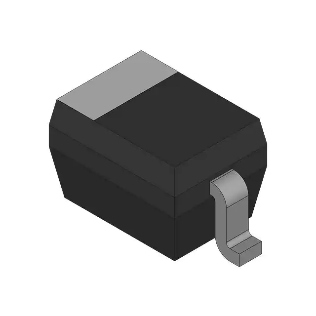
Renesas RKZ3.6B2KG#P6
- Part No.:
- RKZ3.6B2KG#P6
- Manufacturer:
- Renesas
- Category:
- Single Zener Diodes
- Package:
- -
- Datasheet:
-
 RKZ3.6B2KG#P6.pdf
- Description:
- DIODE ZENER
- Quantity:
- Payment:

- Shipping:

Inventory:138,000
Please send an inquiry. Send us your inquiry, and we will respond immediately.
Product details
Overview
RKZ3.6B2KG#P6 from Renesas Electronics is a silicon planar Zener diode designed for surge absorption and voltage stabilization in low-power signal conditioning and protection circuits, with a nominal Zener voltage of 3.6 V (3.55–3.80 V), 10 μA maximum reverse current at 1.0 V, 130 Ω typical dynamic resistance at 5 mA, and 200 mW power dissipation on PCB - deployed in compact consumer sensor interfaces and USB port ESD clamping.
For engineers reviewing the RKZ3.6B2KG#P6 datasheet, RKZ3.6B2KG#P6 pinout, RKZ3.6B2KG#P6 application, or RKZ3.6B2KG#P6 equivalent, this device serves as a halogen-free, Pb-free surface-mount Zener for precision low-voltage regulation and transient suppression where thermal derating above 25°C and ESD robustness (±30 kV per IEC 61000-4-2) are critical selection criteria.
Technical Context
This Zener operates in reverse-biased breakdown mode to maintain stable reference voltage under varying load and temperature conditions. Its ultra-small URP (SC-76A) package enables high-density mounting, and its halogen-free construction complies with JEDEC J-STD-020 moisture sensitivity level 1 requirements.
The device exhibits a negative temperature coefficient near 3.6 V (≈ –0.04 %/°C), confirmed by Fig.2 in REJ03G1512-0300, and supports nonrepetitive surge reverse power up to ~1.2 W for 10 ms (Fig.4), making it suitable for transient overvoltage clamping in low-energy signal paths.
Key Specifications
| Parameter | Value and Actual Design Meaning |
|---|---|
| Zener Voltage (VZ) | 3.55–3.80 V at 5 mA - defines stable clamping threshold for 3.3 V logic rail protection |
| Reverse Current (IR) | ≤10 μA at VR = 1.0 V - ensures minimal leakage in standby mode |
| Dynamic Resistance (rd) | 130 Ω max at IZ = 5 mA - determines voltage regulation stiffness under load variation |
| Power Dissipation (Pd) | 200 mW at Ta = 25°C on PCB - sets absolute thermal limit before derating begins |
| ESD Capability | ±30 kV (HBM, C = 150 pF, R = 330 Ω) - qualifies for direct I/O line protection without external TVS |
| Junction Temperature (Tj) | 150°C max - constrains operating ambient range when mounted on standard FR-4 |
| Package | URP (SC-76A), 2-pin surface-mount - footprint measures 1.70 × 0.90 × 0.45 mm (L×W×H) |
Pinout & Package
Ultra-small Resin Package (URP, JEITA code SC-76A) with 2-terminal surface-mount configuration. Mass: 0.004 g (typ.). Dimensions: 1.70 mm (L) × 0.90 mm (W) × 0.45 mm (H). Cathode marked with band on terminal 1.
| Pin/Terminal | Circuit Role | Design Meaning |
|---|---|---|
| 1 | Cathode | Connected to regulated output node or protected signal line; polarity must be observed for correct clamping direction |
| 2 | Anode | Typically tied to ground or lower-potential reference; forms reverse-bias path during overvoltage events |
Key Features
| Feature | Design Value |
|---|---|
| Halogen-free & Pb-free construction | Complies with RoHS Directive 2011/65/EU and JEDEC J-STD-020 MSL Level 1 - eliminates hazardous substances without compromising solderability |
| Ultra-small URP package | 1.70 × 0.90 mm footprint - enables placement in space-constrained IoT sensor nodes and wearables |
| High ESD immunity | ±30 kV HBM rating - eliminates need for discrete ESD diodes in USB 2.0 D+/D− lines and I²C buses |
| Stable low-voltage Zener | 3.6 V ±3.5% tolerance at 5 mA - provides accurate reference for ADC biasing and comparator thresholds |
| Taped packaging | 3,000 pcs/reel (P taping) - supports automated SMT assembly with zero manual handling |
Applications
| USB 2.0 Data Line Protection | I²C Bus Voltage Clamping |
|---|---|
Use Scenario: Protecting D+ and D− lines against ESD events during hot-plug insertion in portable peripherals. IC Role / Device Role / Timing Role: Bidirectional shunt clamp absorbing transients while maintaining signal integrity below 480 Mbps. Use Value: Prevents latch-up in USB transceivers by clamping excursions to ≤3.8 V, leveraging 30 kV HBM rating and <1 ns response. |
Use Scenario: Stabilizing pull-up voltage on SDA/SCL lines in multi-master embedded systems with mixed-voltage peripherals. IC Role / Device Role / Timing Role: Low-leakage Zener reference ensuring reliable logic-high definition across temperature (≤10 μA at 1.0 V). Use Value: Maintains I²C timing margins by limiting voltage drift to ±0.05 V over –40°C to +85°C ambient. |
| Low-Power Sensor Biasing | Microcontroller Reset Circuit |
Use Scenario: Providing stable 3.3 V bias for analog front-end op-amps in battery-powered environmental sensors. IC Role / Device Role / Timing Role: Precision voltage reference source with 130 Ω dynamic impedance minimizing supply-induced noise coupling. Use Value: Enables sub-10-bit ADC accuracy by holding reference deviation within ±0.1% over 10–100 μA load variation. |
Use Scenario: Generating clean reset threshold for 3.3 V microcontrollers during brown-out conditions. IC Role / Device Role / Timing Role: Zener-based hysteresis element in RC reset generator, triggering reset at 3.55 V and releasing at 3.80 V. Use Value: Eliminates external comparator by exploiting tight VZ tolerance (±3.5%) and predictable temperature coefficient. |
Equivalent & Alternatives
The following parts are listed as comparable options for similar Zener diode applications.
| Alternative Part | Technical Difference | Application Difference | Selection Advice |
|---|---|---|---|
| BZX584-C3V6 | Same nominal VZ (3.6 V), but SOD-323 package (1.7 × 1.3 mm); 250 mW Pd; ±5% tolerance | Higher power margin but larger footprint; less suitable for ultra-dense layouts | Select BZX584-C3V6 only if board space allows 0.4 mm wider body and higher thermal mass is needed |
| MMSZ4685 | VZ = 3.68 V (3.5–3.85 V), SOD-123 package (3.7 × 1.6 mm); 500 mW Pd; no halogen-free guarantee | Higher surge capability but incompatible with lead-free/halogen-free compliance mandates | Choose MMSZ4685 only for non-regulated industrial designs requiring >200 mW continuous dissipation |
Compared with BZX584-C3V6 and MMSZ4685, RKZ3.6B2KG#P6 delivers tighter voltage tolerance (±3.5% vs ±5%), smallest footprint (URP), and guaranteed halogen-free/Pb-free compliance - making it optimal for space- and compliance-critical consumer electronics.
Availability
RKZ3.6B2KG#P6 is available at Aetrix Electronics and suitable for USB interface protection, I²C bus stabilization, and low-power sensor biasing requiring stable component supply, full traceability, and RoHS-compliant sourcing.
Supply support for RKZ3.6B2KG#P6 includes scheduled delivery planning, volume procurement assistance, BOM continuity management, traceable sourcing, and lifecycle availability coordination for OEM customers, industrial embedded developers, connected-device designers, and electronics production programs.
Manufacturer
Renesas Electronics Corporation is a global semiconductor leader specializing in microcontrollers, analog, and power devices for automotive, industrial, and IoT applications.
The RKZ-KG Series targets compact, high-reliability surge absorption and voltage stabilization in portable and battery-powered systems - engineered specifically for halogen-free, high-density SMT deployment.
FAQ
What is the Zener voltage tolerance of RKZ3.6B2KG#P6 at 5 mA?
The RKZ3.6B2KG#P6 has a Zener voltage range of 3.55 V to 3.80 V at 5 mA test current, corresponding to ±3.5% tolerance about the nominal 3.6 V value. This tight tolerance is specified in the Electrical Characteristics table on page 2 of REJ03G1512-0300 and enables precise voltage clamping without additional trimming components in RKZ3.6B2KG#P6-based designs.
Does RKZ3.6B2KG#P6 meet RoHS and halogen-free requirements?
Yes, RKZ3.6B2KG#P6 is explicitly designated as a halogen-free and Pb-free part (RKZ-KG-P6 Series), compliant with EU RoHS Directive 2011/65/EU. The "P6" suffix confirms full conformance, and the device carries no brominated flame retardants or chlorine-based compounds - verified in the Features section and Ordering Information table of REJ03G1512-0300 for RKZ3.6B2KG#P6.
What is the maximum allowable ambient temperature for RKZ3.6B2KG#P6 at full 200 mW power dissipation?
RKZ3.6B2KG#P6 achieves its full 200 mW rated power dissipation only at Ta = 25°C. As shown in Fig.3 (Power Dissipation vs. Ambient Temperature), derating begins linearly above 25°C, reaching zero dissipation at approximately 150°C. For continuous operation at 200 mW, ambient temperature must remain at or below 25°C - a key thermal constraint in RKZ3.6B2KG#P6 layout planning.
How is the cathode identified on the RKZ3.6B2KG#P6 package?
The cathode of RKZ3.6B2KG#P6 is marked with a visible band on terminal 1, consistent with the Pin Arrangement diagram on page 1 of REJ03G1512-0300. The laser mark "3 • 6" appears adjacent to this band, confirming orientation. Correct polarity is essential: cathode connects to the protected signal line, anode to ground - misorientation renders RKZ3.6B2KG#P6 ineffective for reverse-transient clamping.
What ESD test standard does the 30 kV rating for RKZ3.6B2KG#P6 follow?
The ±30 kV ESD capability of RKZ3.6B2KG#P6 is measured per Human Body Model (HBM) per JEDEC JS-001, using C = 150 pF and R = 330 Ω, with 10 pulses applied in both forward and reverse directions. This specification is documented in the Electrical Characteristics table (page 2) and Notes section of REJ03G1512-0300 - confirming RKZ3.6B2KG#P6's suitability for direct I/O line protection without supplemental ESD components.
RKZ3.6B2KG#P6 Specifications
- Product attributes
- Attribute value
- Manufacturer:
- Renesas
- Series:
- *
- Package/Case:
- -
- Packaging:
- Bulk
- Product Status:
- Active
- Voltage - Zener (Nom) (Vz):
- -
- Tolerance:
- -
- Power - Max:
- -
- Impedance (Max) (Zzt):
- -
- Current - Reverse Leakage @ Vr:
- -
- Voltage - Forward (Vf) (Max) @ If:
- -
- Operating Temperature:
- -
- Grade:
- -
- Qualification:
- -
- Mounting Type:
- -
- Supplier Device Package:
- -
RKZ3.6B2KG#P6 FAQ
1.How can I place an order for RKZ3.6B2KG#P6 through Aetrix?
Please submit a Request for Quotation (RFQ) for RKZ3.6B2KG#P6 on Aetrix. Our sales agent will provide a competitive quotation and guide you through the order confirmation once you accept the terms.
2.Are the price and stock information for RKZ3.6B2KG#P6 reliable?
The price and inventory of RKZ3.6B2KG#P6 are updated periodically and may fluctuate due to market conditions. Stock and pricing data are typically refreshed every 24 hours. Quotation validity for RKZ3.6B2KG#P6 is usually 5 days.
3.What payment methods are accepted for RKZ3.6B2KG#P6?
We accept Wire Transfer, PayPal, Credit Card, Western Union, MoneyGram, and Escrow for RKZ3.6B2KG#P6 transactions.
Note: Certain payment methods may incur a processing fee.
4.How is shipping managed for RKZ3.6B2KG#P6?
RKZ3.6B2KG#P6 orders can be shipped via leading logistics carriers, including DHL, UPS, FedEx, TNT, or Registered Mail.
Once your RKZ3.6B2KG#P6 order is processed, you will receive an email with the shipment details and tracking number.
Note: Tracking information may take up to 24 hours to appear. Express delivery typically takes 3–5 business days.
5.How can I obtain technical support or documentation for RKZ3.6B2KG#P6?
For technical support, including RKZ3.6B2KG#P6 datasheets, pinout diagrams, or application guidance, please contact our engineering support team. They can provide detailed documentation and assistance for your RKZ3.6B2KG#P6 requirements.
6.How does Aetrix verify that RKZ3.6B2KG#P6 is sourced from the original manufacturer or authorized distributors?
All RKZ3.6B2KG#P6 products on Aetrix are procured from qualified distributors and authorized channels. Our dedicated quality assurance team conducts strict verification, including traceability checks and, if necessary, third-party testing. This ensures that RKZ3.6B2KG#P6 meets industry standards.
7.What is the process for return or replacement of RKZ3.6B2KG#P6?
All RKZ3.6B2KG#P6 units undergo pre-shipment inspection (PSI). If there is an issue with RKZ3.6B2KG#P6, returns or replacements are accepted under the following conditions:
1.Quantity discrepancies, incorrect items, or visible external defects (such as breakage or corrosion), acknowledged by Aetrix.
2.The issue is reported within 90 days of delivery.
3.The RKZ3.6B2KG#P6 part is unused and in its original packaging.
Return procedure for RKZ3.6B2KG#P6:
1.Submit a request within 90 days.
2.Obtain a Return Material Authorization (RMA) from Aetrix.
RKZ3.6B2KG#P6 Tags
-
MMBZ5240B-7-F
Diodes Incorporated
-
BZT52C5V6T-7
Diodes Incorporated
-
MMSZ5231B-7-F
Diodes Incorporated
-
BZT52C15-7-F
Diodes Incorporated
-
BZX84C3V3LT1G
onsemi
-
MMSZ5245BS-7-F
Diodes Incorporated
-
MMSZ4682T1G
onsemi
-
BZT52C15S-7-F
Diodes Incorporated
-
MM5Z5V1ST1G
onsemi
-
SMAJ4744A-TP
Micro Commercial Co
-
BZT52C3V6LP-7
Diodes Incorporated
-
SMAZ12-13-F
Diodes Incorporated
Tech Hub

TTL and CMOS logic families differ in thresholds, loading, output drive, power and timing. This engineering guide compares 74HC and 74HCT, calculates noise margins and checks 3.3 V/5 V compatibility.

A practical engineering guide to 3.3V and 5V logic compatibility, input thresholds, resistor dividers, translator ICs, MOSFET level shifting, I2C pull-ups, timing limits and power-sequencing risks.

The 74HC595 uses push-pull logic outputs, while the TPIC6B595 uses 50 V open-drain DMOS sinks for higher-power loads. This guide compares timing, current limits, 3.3 V interfacing, load wiring, thermal…

The 74HC595 converts serial data into eight stable parallel outputs. This guide covers pin functions, shift and storage timing, OE and MR behavior, drive-current limits, cascading, voltage compatibilit…

A technical comparison of level-sensitive latches and edge-triggered flip-flops, covering timing windows, setup and hold limits, master–slave operation, time borrowing, race-through, HDL inference and…

A D latch stores one bit while Enable controls when data can pass. This reference covers gate-level operation, truth tables, transparency, setup and hold timing, LE versus OE, common ICs and practical …

An SR latch stores one bit through cross-coupled feedback. This engineering reference covers NOR and NAND implementations, truth tables, forbidden-state recovery, gated operation, switch debouncing, fa…

Latch circuits retain one bit through feedback. This technical reference covers SR and D latches, truth tables, transparency, timing limits, latch-versus-flip-flop behavior, applications and common log…

An engineering guide to LED driver operation, constant-current and constant-voltage outputs, linear and switching topologies, dimming, IC selection, calculations, replacement compatibility, and fault c…

Operational amplifier guide covering op amp basics, feedback, ideal vs real op amps, common configurations, buffer circuits, offset, bias current, gain-bandwidth, slew rate, rail-to-rail limits and sel…


