
 My Inquiry
 My Account


Renesas RMLV0816BGSD-4S2#AA1
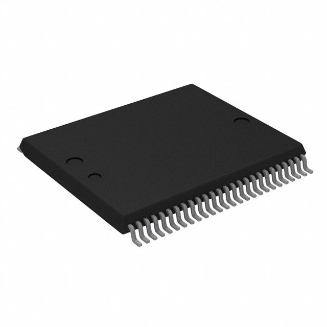
- Part No.:
- RMLV0816BGSD-4S2#AA1
- Manufacturer:
- Renesas
- Category:
- Memory
- Package:
- 52-TFSOP (0.350", 8.89mm Width)
- Datasheet:
-
 RMLV0816BGSD-4S2#AA1.pdf
- Description:
- IC SRAM 8MBIT PARALLEL 52TSOP II
- Quantity:
- Payment:

- Shipping:

Inventory:205
Please send an inquiry. Send us your inquiry, and we will respond immediately.
Product details
Overview
RMLV0816BGSD-4S2 from Renesas Electronics is an 8Mb Advanced LPSRAM organized as 524,288-word × 16-bit (or 1,048,576-word × 8-bit), operating from a single 2.4V–3.6V supply, with 45ns max access time at 2.7–3.6V and 0.45µA typical standby current at 25°C - designed for low-power embedded systems requiring battery-backed memory retention.
For engineers reviewing the RMLV0816BGSD-4S2 datasheet, RMLV0816BGSD-4S2 pinout, RMLV0816BGSD-4S2 application, or RMLV0816BGSD-4S2 equivalent, key selection criteria include byte/word mode flexibility, µTSOP (II) package compatibility, TTL-level I/O interface, and verified data retention down to 1.5V.
Technical Context
This static RAM implements dual-mode addressing (A0–A18 for word mode; A–1–A18 for byte mode) with independent upper/lower byte control via UB# and LB#, enabling precise 8-bit or 16-bit data transfers without external logic. Its three-state DQ0–DQ15 bus supports direct TTL-compatible interfacing with microcontrollers and ASICs.
The device uses Renesas's Advanced LPSRAM process to achieve simultaneous low active power (25mA typ. at 45ns cycle) and ultra-low standby current (0.45µA typ.), with multiple data retention entry paths (CS1#, CS2, or LB#/UB# assertion) and guaranteed operation across –40°C to +85°C.
Key Specifications
| Parameter | Value and Actual Design Meaning |
|---|---|
| Memory capacity | 8 Mbit (524,288 × 16 or 1,048,576 × 8) - supports flexible word/byte system architectures |
| Supply voltage | 2.4V to 3.6V - single-supply operation compatible with 3V logic families and battery-backed systems |
| Access time | 45 ns max (2.7–3.6V); 55 ns max (2.4–2.7V) - defines minimum read/write cycle timing for host controller design |
| Standby current | 0.45 µA typ. at 25°C - enables multi-year battery backup in always-on embedded applications |
| Data retention VCC | 1.5V min - maintains stored data during brown-out or backup power transitions |
| Operating temperature | –40°C to +85°C - qualified for industrial and automotive under-hood environments |
| Package | 52-pin µTSOP (II), 10.79mm × 10.49mm - surface-mount footprint compatible with high-density PCB layouts |
Pinout & Package
52-pin plastic µTSOP (II) package with standard JEDEC-compliant footprint and lead pitch of 0.5mm.
| Pin/Terminal | Circuit Role | Design Meaning |
|---|---|---|
| VCC | Power supply | Primary 2.4–3.6V supply rail; decoupling required within 5mm |
| VSS | Ground | Digital ground reference for all I/O and internal circuitry |
| A0–A18 | Address input (word mode) | 19-bit address bus for 524,288-word × 16-bit configuration |
| A–1–A18 | Address input (byte mode) | 19-bit address bus with A–1 enabling 1M-word × 8-bit mapping |
| DQ0–DQ15 | Data input/output | Bidirectional 16-bit data bus with three-state output control |
| CS1#, CS2 | Chip select inputs | Active-low hierarchical chip enable; CS2 controls buffer activation and retention mode |
| OE#, WE# | Output and write enable | Separate controls for read (OE#) and write (WE#) cycles; both active-low |
| LB#, UB# | Byte select | Independent lower/upper byte gating for 8-bit sub-accesses in 16-bit bus systems |
| BYTE# | Byte mode enable | Configures address decoding and DQ behavior for byte vs. word operation |
| NC | No connection | Unbonded pins; must be left floating or tied to VSS per layout guidelines |
Key Features
| Feature | Design Value |
|---|---|
| Single 3V supply operation | Eliminates need for dual-voltage rails or level shifters in 3V system designs |
| Direct TTL compatibility | All inputs and outputs meet TTL voltage thresholds, enabling seamless interface with legacy microcontrollers |
| Multi-path data retention | Three independent entry methods (CS1#, CS2, or LB#/UB# assertion) simplify low-power state management |
| Equal access and cycle times | Removes timing margin uncertainty between read and write operations in real-time firmware |
| Common I/O bus with three-state control | Reduces PCB trace count and simplifies bus arbitration in shared-memory architectures |
Applications
| Industrial PLC Data Buffer | Medical Device Parameter Storage |
|---|---|
Use Scenario: Real-time logging of sensor readings and control states in programmable logic controllers during mains power interruption. IC Role / Device Role / Timing Role: Nonvolatile data buffer maintaining critical operational history using battery-backed retention mode. Use Value: Guarantees 0.45µA standby current and 1.5V data retention voltage, extending coin-cell life beyond 5 years. |
Use Scenario: Storing calibration coefficients and patient-specific settings in portable diagnostic equipment with intermittent power. IC Role / Device Role / Timing Role: Low-latency, byte-selectable SRAM for fast parameter recall during boot and runtime reconfiguration. Use Value: 45ns access time and LB#/UB# control enable deterministic <100ns parameter fetch without software overhead. |
| Automotive Infotainment Cache | Network Edge Router Packet Buffer |
Use Scenario: Caching UI assets and navigation map tiles in head-unit systems exposed to wide ambient temperature swings. IC Role / Device Role / Timing Role: High-reliability, temperature-hardened memory supporting –40°C to +85°C operation without derating. Use Value: Qualified industrial temperature range and 52-pin µTSOP (II) package ensure mechanical stability under thermal cycling. |
Use Scenario: Temporary storage of fragmented Ethernet frames in small-form-factor industrial routers with space-constrained PCBs. IC Role / Device Role / Timing Role: Compact, low-power SRAM providing 16-bit parallel access to accelerate frame assembly/disassembly. Use Value: 10.79mm × 10.49mm µTSOP (II) footprint saves >30% board area versus SOIC alternatives while maintaining 8Mb density. |
Equivalent & Alternatives
The following parts are listed as comparable options for similar low-power SRAM applications.
| Alternative Part | Technical Difference | Application Difference | Selection Advice |
|---|---|---|---|
| IS61LV25616AL-10TLI | 10ns faster access (35ns), but 5µA typical standby current - 11× higher than RMLV0816BGSD-4S2 | Preferred where speed dominates over battery life; unsuitable for multi-year backup | Select only when system clock budget requires sub-40ns latency and power constraints are secondary |
| AS6C4008-55ZIN | Same 45ns access and 52-pin TSOP-II package, but 2.7–3.6V supply only (no 2.4V support) | Lacks low-voltage operation needed for brown-out resilience and wide-input DC-DC designs | Use if supply is tightly regulated ≥2.7V and data retention below 2.4V is not required |
Compared with IS61LV25616AL-10TLI and AS6C4008-55ZIN, the RMLV0816BGSD-4S2 uniquely balances ultra-low standby current (0.45µA), extended 2.4V–3.6V supply range, and industrial temperature rating - making it optimal for battery-critical, wide-input, and thermally demanding deployments.
Availability
RMLV0816BGSD-4S2 is available at Aetrix Electronics and suitable for industrial PLC data buffering, medical device parameter storage, and automotive infotainment caching requiring stable component supply across long production lifecycles.
Supply support for RMLV0816BGSD-4S2 includes scheduled delivery planning, volume procurement assistance, BOM continuity management, traceable sourcing, and lifecycle availability coordination for OEM customers, industrial embedded developers, connected-device designers, and electronics production programs.
Manufacturer
Renesas Electronics Corporation is a global semiconductor leader specializing in microcontrollers, analog, power, and memory solutions for industrial, automotive, and infrastructure markets.
The RMLV0816BGSD-4S2 belongs to Renesas's Advanced LPSRAM product line, engineered specifically for ultra-low-power, battery-backed memory applications in space- and energy-constrained embedded systems.
FAQ
What is the minimum supply voltage required for data retention in RMLV0816BGSD-4S2?
The RMLV0816BGSD-4S2 guarantees data retention down to 1.5V VCC when placed in standby mode via CS1#, CS2, or LB#/UB# assertion. This allows continued memory integrity during brown-out conditions or coin-cell backup operation, with typical retention current of 0.45µA at 25°C and 3.0V supply.
Does RMLV0816BGSD-4S2 support both 8-bit and 16-bit data bus configurations?
Yes, the RMLV0816BGSD-4S2 supports dual organization: 524,288-word × 16-bit (using A0–A18) or 1,048,576-word × 8-bit (using A–1–A18). The BYTE# pin selects mode, and LB#/UB# enable independent byte access - eliminating need for external multiplexing logic.
What is the maximum operating current of RMLV0816BGSD-4S2 during active read/write cycles?
The RMLV0816BGSD-4S2 draws up to 25mA typical ICC1 current at 45ns cycle time (VCC = 3.0V, Ta = 25°C), and 30mA maximum. At slower 55ns cycles (2.4–2.7V), typical current is 20mA. These values include all internal buffers and array activity under full bus loading.
Can RMLV0816BGSD-4S2 be used with 5V-tolerant microcontrollers?
No - the RMLV0816BGSD-4S2 is strictly a 3V-family device with VIH = 2.2V (min) at 2.4–2.7V supply and 2.4V (min) at 2.7–3.6V. It is not 5V-tolerant; direct connection to 5V logic requires level translation to avoid damage and ensure signal integrity.
Is the 52-pin µTSOP (II) package of RMLV0816BGSD-4S2 RoHS compliant and lead-free?
Yes, the RMLV0816BGSD-4S2 is manufactured in a lead-free, RoHS-compliant 52-pin µTSOP (II) package per Renesas documentation R10DS0253EJ0201 Rev.2.01. The package uses matte tin plating and meets JEDEC J-STD-020 moisture sensitivity level 3 (MSL3) requirements.
RMLV0816BGSD-4S2#AA1 Specifications
- Product attributes
- Attribute value
- Manufacturer:
- Renesas
- Series:
- -
- Package/Case:
- 52-TFSOP (0.350", 8.89mm Width)
- Packaging:
- Tray
- Product Status:
- Active
- Programmable:
- Not Verified
- Memory Type:
- Volatile
- Memory Format:
- SRAM
- Technology:
- SRAM
- Memory Size:
- 8Mbit
- Memory Organization:
- 1M x 8, 512K x 16
- Memory Interface:
- Parallel
- Clock Frequency:
- -
- Write Cycle Time - Word, Page:
- 45ns
- Access Time:
- 45 ns
- Voltage - Supply:
- 2.4V ~ 3.6V
- Operating Temperature:
- -40°C ~ 85°C (TA)
- Grade:
- -
- Qualification:
- -
- Mounting Type:
- Surface Mount
- Supplier Device Package:
- 52-TSOP II
RMLV0816BGSD-4S2#AA1 FAQ
1.How can I place an order for RMLV0816BGSD-4S2#AA1 through Aetrix?
Please submit a Request for Quotation (RFQ) for RMLV0816BGSD-4S2#AA1 on Aetrix. Our sales agent will provide a competitive quotation and guide you through the order confirmation once you accept the terms.
2.Are the price and stock information for RMLV0816BGSD-4S2#AA1 reliable?
The price and inventory of RMLV0816BGSD-4S2#AA1 are updated periodically and may fluctuate due to market conditions. Stock and pricing data are typically refreshed every 24 hours. Quotation validity for RMLV0816BGSD-4S2#AA1 is usually 5 days.
3.What payment methods are accepted for RMLV0816BGSD-4S2#AA1?
We accept Wire Transfer, PayPal, Credit Card, Western Union, MoneyGram, and Escrow for RMLV0816BGSD-4S2#AA1 transactions.
Note: Certain payment methods may incur a processing fee.
4.How is shipping managed for RMLV0816BGSD-4S2#AA1?
RMLV0816BGSD-4S2#AA1 orders can be shipped via leading logistics carriers, including DHL, UPS, FedEx, TNT, or Registered Mail.
Once your RMLV0816BGSD-4S2#AA1 order is processed, you will receive an email with the shipment details and tracking number.
Note: Tracking information may take up to 24 hours to appear. Express delivery typically takes 3–5 business days.
5.How can I obtain technical support or documentation for RMLV0816BGSD-4S2#AA1?
For technical support, including RMLV0816BGSD-4S2#AA1 datasheets, pinout diagrams, or application guidance, please contact our engineering support team. They can provide detailed documentation and assistance for your RMLV0816BGSD-4S2#AA1 requirements.
6.How does Aetrix verify that RMLV0816BGSD-4S2#AA1 is sourced from the original manufacturer or authorized distributors?
All RMLV0816BGSD-4S2#AA1 products on Aetrix are procured from qualified distributors and authorized channels. Our dedicated quality assurance team conducts strict verification, including traceability checks and, if necessary, third-party testing. This ensures that RMLV0816BGSD-4S2#AA1 meets industry standards.
7.What is the process for return or replacement of RMLV0816BGSD-4S2#AA1?
All RMLV0816BGSD-4S2#AA1 units undergo pre-shipment inspection (PSI). If there is an issue with RMLV0816BGSD-4S2#AA1, returns or replacements are accepted under the following conditions:
1.Quantity discrepancies, incorrect items, or visible external defects (such as breakage or corrosion), acknowledged by Aetrix.
2.The issue is reported within 90 days of delivery.
3.The RMLV0816BGSD-4S2#AA1 part is unused and in its original packaging.
Return procedure for RMLV0816BGSD-4S2#AA1:
1.Submit a request within 90 days.
2.Obtain a Return Material Authorization (RMA) from Aetrix.
RMLV0816BGSD-4S2#AA1 Tags

-
M24C02-WMN6TP
STMicroelectronics

-
AT24C02C-XHM-T
Microchip Technology

-
AT21CS01-STUM10-T
Microchip Technology

-
AT24C02C-SSHM-T
Microchip Technology

-
24LC01BT-I/OT
Microchip Technology

-
M24C02-FMC6TG
STMicroelectronics
-
AT24CS02-SSHM-T
Microchip Technology

-
93LC46BT-I/OT
Microchip Technology
-
AT24C04C-SSHM-T
Microchip Technology

-
24LC01BT-I/SN
Microchip Technology
-
24AA02UIDT-I/OT
Microchip Technology

-
AT24C08C-STUM-T
Microchip Technology
Tech Hub

TTL and CMOS logic families differ in thresholds, loading, output drive, power and timing. This engineering guide compares 74HC and 74HCT, calculates noise margins and checks 3.3 V/5 V compatibility.

A practical engineering guide to 3.3V and 5V logic compatibility, input thresholds, resistor dividers, translator ICs, MOSFET level shifting, I2C pull-ups, timing limits and power-sequencing risks.

The 74HC595 uses push-pull logic outputs, while the TPIC6B595 uses 50 V open-drain DMOS sinks for higher-power loads. This guide compares timing, current limits, 3.3 V interfacing, load wiring, thermal…

The 74HC595 converts serial data into eight stable parallel outputs. This guide covers pin functions, shift and storage timing, OE and MR behavior, drive-current limits, cascading, voltage compatibilit…

A technical comparison of level-sensitive latches and edge-triggered flip-flops, covering timing windows, setup and hold limits, master–slave operation, time borrowing, race-through, HDL inference and…

A D latch stores one bit while Enable controls when data can pass. This reference covers gate-level operation, truth tables, transparency, setup and hold timing, LE versus OE, common ICs and practical …

An SR latch stores one bit through cross-coupled feedback. This engineering reference covers NOR and NAND implementations, truth tables, forbidden-state recovery, gated operation, switch debouncing, fa…

Latch circuits retain one bit through feedback. This technical reference covers SR and D latches, truth tables, transparency, timing limits, latch-versus-flip-flop behavior, applications and common log…

An engineering guide to LED driver operation, constant-current and constant-voltage outputs, linear and switching topologies, dimming, IC selection, calculations, replacement compatibility, and fault c…

Operational amplifier guide covering op amp basics, feedback, ideal vs real op amps, common configurations, buffer circuits, offset, bias current, gain-bandwidth, slew rate, rail-to-rail limits and sel…


