
 My Inquiry
 My Account


Infineon Technologies S29PL032J60BFW123
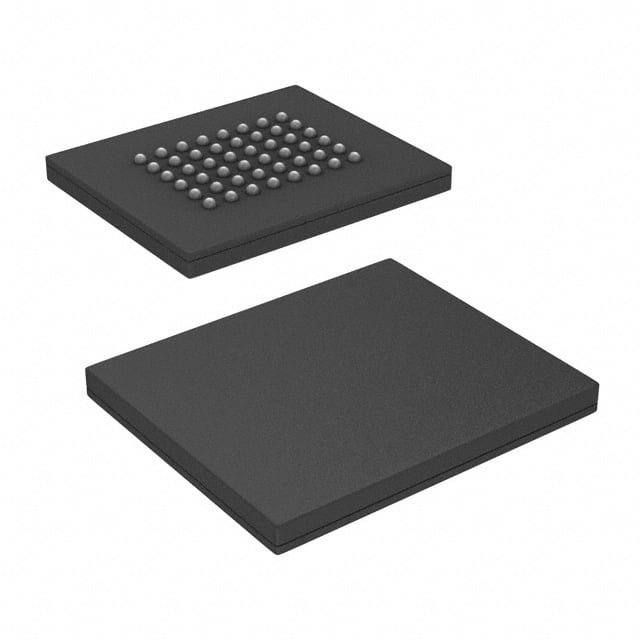
- Part No.:
- S29PL032J60BFW123
- Manufacturer:
- Infineon Technologies
- Category:
- Memory
- Package:
- 48-VFBGA
- Datasheet:
-
 S29PL032J60BFW123.pdf
- Description:
- IC FLASH 32MBIT PARALLEL 48FBGA
- Quantity:
- Payment:

- Shipping:

Inventory:1,667
Please send an inquiry. Send us your inquiry, and we will respond immediately.
Product details
Overview
S29PL032J60BFW123 from Infineon Technologies (formerly Cypress) is a 32-Mbit (2 M × 16-bit), 3.0 V-only Page Mode Flash memory with FlexBank architecture, Enhanced VersatileI/O™, and simultaneous read/write operation across four independent banks. It delivers 20 ns page access, 55 ns random access, 1 million erase/program cycles per sector, and 20-year data retention - deployed in industrial control firmware storage where deterministic bank-switching and in-system reprogramming are required.
For engineers reviewing the S29PL032J60BFW123 datasheet, S29PL032J60BFW123 pinout, S29PL032J60BFW123 application, or S29PL032J60BFW123 equivalent, key selection criteria include 48-ball Fine-pitch BGA (VBK048) package compatibility, 2.7–3.6 V single-supply operation, CFI compliance, persistent/password sector protection, and zero-latency bank switching for real-time firmware updates.
Technical Context
This device implements a 4-bank FlexBank architecture enabling concurrent read from one bank while erasing or programming another - eliminating latency between host command execution and data availability. Each bank supports independent sector erase (4 Kword sectors), with Bank A and D sized at 4 Mbit (4 Kw × 8 + 32 Kw × 7) and Banks B/C at 12 Mbit (32 Kw × 24) for asymmetric firmware partitioning.
Enhanced VersatileI/O™ fixes I/O voltage tolerance and output drive to VIO = 3.0 V, ensuring signal integrity across mixed-voltage systems without level shifters. Sector protection is enforced via three mechanisms: hardware WP# pin lock for top/bottom boot blocks, persistent PPB bits for permanent in-system locking, and 64-bit password-secured regions requiring authenticated unlock sequences before modification.
Key Specifications
| Parameter | Value and Actual Design Meaning |
|---|---|
| Memory Density | 32 Mbit (2 Mwords × 16-bit bus), enabling compact firmware images up to 4 MB in x16 configuration |
| Access Time | 20 ns page mode / 55 ns random access - meets real-time boot latency requirements for embedded controllers |
| Voltage Range | 2.7–3.6 V single supply - supports battery-backed and wide-input industrial power rails without auxiliary regulators |
| Endurance | 1 million program/erase cycles per sector - validated for field-upgradable firmware with daily update cycles over 27 years |
| Data Retention | 20 years at 125°C - qualified for extended-life automotive and industrial deployments without refresh |
| Package | 8.15 × 6.15 mm, 48-ball Fine-pitch BGA (VBK048) - enables high-density PCB layouts with 0.5 mm pitch routing |
| CFI Compliance | JEDEC 42.4-compliant Common Flash Interface - allows automatic runtime detection and driver configuration in Linux/U-Boot environments |
Pinout & Package
Package: 48-ball Fine-pitch BGA (VBK048), 8.15 mm × 6.15 mm, 0.5 mm ball pitch, RoHS-compliant.
| Pin/Terminal | Circuit Role | Design Meaning |
|---|---|---|
| A0–A20 | Address Inputs | 21-bit address bus supporting full 2 Mword addressing; A0–A1 select byte within 16-bit word |
| DQ0–DQ15 | Data I/O | 16-bit bidirectional data bus with VIO-referenced drive strength and input thresholds |
| CE#, OE#, WE# | Chip/Output/Write Enable | Standard asynchronous control signals; all active-low with setup/hold timing referenced to VIO |
| RY/BY# | Ready/Busy Output | Open-drain status indicator: low during erase/program, high when ready for next command or read |
| RESET# | Hardware Reset | Asynchronous reset that forces device into reading array state, clearing internal state machines |
| WP#/ACC | Write Protect/Acceleration | VIL = permanent lock of boot sectors; VIH = unlock; VHH = factory accelerated programming mode |
| VIO | I/O Voltage Reference | 3.0 V reference setting I/O logic levels and drive strength - no external level translation needed |
Key Features
| Feature | Design Value |
|---|---|
| FlexBank Architecture | Four independent banks (A–D) allow concurrent read from one bank while erasing/programming another - eliminates CPU idle time during firmware updates |
| Enhanced VersatileI/O™ | VIO = 3.0 V ensures consistent I/O thresholds and drive strength across temperature and voltage - removes need for external level shifters in mixed-voltage SoC interfaces |
| Password Sector Protection | 64-bit user-defined password required to unlock protected sectors - prevents unauthorized firmware modification in field-deployed devices |
| Secured Silicon Sector | 128-word region (64 factory-locked + 64 customer-lockable) stores cryptographic keys or calibration data immune to bulk erase |
| CFI Compliance | Standardized JEDEC 42.4 interface provides runtime-accessible device geometry, timing, and command set metadata - enables generic flash drivers |
Applications
| Industrial PLC Firmware Storage | Automotive ADAS Boot Memory |
|---|---|
Use Scenario: Storing and updating ladder logic and motion control firmware in programmable logic controllers operating in harsh factory environments. IC Role / Device Role / Timing Role: Non-volatile code storage with in-system reprogrammability and hardware write protection against EMI-induced corruption. Use Value: Persistent sector protection prevents accidental overwrite of critical boot code during field updates; 20-year retention ensures lifetime firmware integrity without replacement. | Use Scenario: Holding boot code and safety-critical sensor fusion algorithms for camera/radar ECUs requiring ASIL-B compliance. IC Role / Device Role / Timing Role: Primary boot memory mapped to ARM Cortex-R5 processor with zero-latency bank switching during OTA firmware validation. Use Value: Simultaneous read/write allows background signature verification in Bank A while executing current firmware from Bank B - no system stall during secure update. |
| Medical Imaging System Configuration | Telecom Base Station FPGA Bitstream |
Use Scenario: Storing calibrated imaging parameters and regulatory-certified DICOM profiles in portable ultrasound devices with battery backup. IC Role / Device Role / Timing Role: Secure parameter storage with password-protected access to prevent unauthorized calibration changes. Use Value: Secured Silicon Sector holds factory-calibrated ADC offsets and gamma tables; 64-bit password ensures only authorized service tools can modify values. | Use Scenario: Storing dual FPGA configuration bitstreams (active/backup) in 5G remote radio units requiring hot-swap reconfiguration. IC Role / Device Role / Timing Role: Dual-bank bitstream storage enabling fail-safe FPGA reload without service interruption. Use Value: FlexBank architecture allows loading new bitstream into Bank C while executing from Bank A - achieves sub-100 ms switchover during network maintenance windows. |
Equivalent & Alternatives
The following parts are listed as comparable options for similar Flash memory applications.
| Alternative Part | Technical Difference | Application Difference | Selection Advice |
|---|---|---|---|
| S29GL032N90TFI020 | 48-ball BGA, 32 Mbit, 90 ns random access, no simultaneous read/write, legacy CFI | Lacks FlexBank and zero-latency switching - unsuitable for real-time firmware update scenarios | Select only if cost sensitivity outweighs performance and update flexibility requirements |
| MX29GL320EHTI-90G | 48-ball BGA, 32 Mbit, 90 ns access, no password protection, no secured silicon sector | Missing hardware-based security features - requires external authentication logic for secure boot | Choose when basic firmware storage suffices and cryptographic isolation is handled externally |
Compared with S29GL032N90TFI020 and MX29GL320EHTI-90G, the S29PL032J60BFW123 uniquely delivers concurrent bank operation, password-secured sectors, and 20 ns page access - making it the only option among the three qualified for deterministic, secure, real-time firmware updates in safety-critical systems.
Availability
S29PL032J60BFW123 is available at Aetrix Electronics and suitable for industrial PLC firmware storage, automotive ADAS boot memory, and medical imaging system configuration requiring stable component supply, long-term lifecycle support, and guaranteed traceable sourcing.
Supply support for S29PL032J60BFW123 includes scheduled delivery planning, volume procurement assistance, BOM continuity management, traceable sourcing, and lifecycle availability coordination for OEM customers, industrial embedded developers, connected-device designers, and electronics production programs.
Manufacturer
Infineon Technologies is a German semiconductor leader specializing in power management, sensing, and memory solutions for industrial, automotive, and IoT applications.
The S29PL-J series was designed specifically for high-reliability embedded systems requiring deterministic firmware update capability, hardware-enforced security, and extended temperature operation - targeting mission-critical control and safety applications.
FAQ
Does S29PL032J60BFW123 support true simultaneous read/write across different banks?
Yes. The FlexBank architecture enables full concurrency: while erasing or programming sectors in Bank A, the host may simultaneously read from any address in Bank B, C, or D with zero latency. This is verified by the device's RY/BY# pin behavior and documented timing diagrams in Section 20.5 of the datasheet.
What is the function of the VIO pin, and can it be tied to VCC?
The VIO pin sets I/O voltage thresholds and drive strength. For S29PL032J, VIO must be 3.0 V - it is internally regulated and cannot be omitted or tied directly to VCC without verifying voltage tolerance. The datasheet specifies VIO = 2.7–3.6 V, but operation outside 3.0 V ±0.1 V degrades timing margins and toggle-bit reliability.
How does Password Sector Protection differ from Persistent Sector Protection?
Persistent Protection uses one-time-programmable PPB bits locked permanently after setting; Password Protection requires presenting a valid 64-bit value before unlocking - allowing dynamic reconfiguration in the field. Both coexist: password-protected sectors remain inaccessible even if PPB bits are set, adding defense-in-depth.
Is the Secured Silicon Sector accessible after factory programming?
Yes. The 128-word Secured Silicon Sector remains fully accessible via the documented command sequence (Section 15.4), but only after entering the correct unlock sequence. Factory-locked words (first 64) cannot be modified; customer-lockable words (next 64) may be permanently locked using the PPB mechanism.
S29PL032J60BFW123 Specifications
- Product attributes
- Attribute value
- Manufacturer:
- Infineon Technologies
- Series:
- PL-J
- Package/Case:
- 48-VFBGA
- Packaging:
- Tape & Reel (TR)
- Product Status:
- Obsolete
- Programmable:
- Not Verified
- Memory Type:
- Non-Volatile
- Memory Format:
- FLASH
- Technology:
- FLASH - NOR
- Memory Size:
- 32Mbit
- Memory Organization:
- 2M x 16
- Memory Interface:
- Parallel
- Clock Frequency:
- -
- Write Cycle Time - Word, Page:
- 60ns
- Access Time:
- 60 ns
- Voltage - Supply:
- 2.7V ~ 3.6V
- Operating Temperature:
- -25°C ~ 85°C (TA)
- Grade:
- -
- Qualification:
- -
- Mounting Type:
- Surface Mount
- Supplier Device Package:
- 48-FBGA (8.15x6.15)
S29PL032J60BFW123 FAQ
1.How can I place an order for S29PL032J60BFW123 through Aetrix?
Please submit a Request for Quotation (RFQ) for S29PL032J60BFW123 on Aetrix. Our sales agent will provide a competitive quotation and guide you through the order confirmation once you accept the terms.
2.Are the price and stock information for S29PL032J60BFW123 reliable?
The price and inventory of S29PL032J60BFW123 are updated periodically and may fluctuate due to market conditions. Stock and pricing data are typically refreshed every 24 hours. Quotation validity for S29PL032J60BFW123 is usually 5 days.
3.What payment methods are accepted for S29PL032J60BFW123?
We accept Wire Transfer, PayPal, Credit Card, Western Union, MoneyGram, and Escrow for S29PL032J60BFW123 transactions.
Note: Certain payment methods may incur a processing fee.
4.How is shipping managed for S29PL032J60BFW123?
S29PL032J60BFW123 orders can be shipped via leading logistics carriers, including DHL, UPS, FedEx, TNT, or Registered Mail.
Once your S29PL032J60BFW123 order is processed, you will receive an email with the shipment details and tracking number.
Note: Tracking information may take up to 24 hours to appear. Express delivery typically takes 3–5 business days.
5.How can I obtain technical support or documentation for S29PL032J60BFW123?
For technical support, including S29PL032J60BFW123 datasheets, pinout diagrams, or application guidance, please contact our engineering support team. They can provide detailed documentation and assistance for your S29PL032J60BFW123 requirements.
6.How does Aetrix verify that S29PL032J60BFW123 is sourced from the original manufacturer or authorized distributors?
All S29PL032J60BFW123 products on Aetrix are procured from qualified distributors and authorized channels. Our dedicated quality assurance team conducts strict verification, including traceability checks and, if necessary, third-party testing. This ensures that S29PL032J60BFW123 meets industry standards.
7.What is the process for return or replacement of S29PL032J60BFW123?
All S29PL032J60BFW123 units undergo pre-shipment inspection (PSI). If there is an issue with S29PL032J60BFW123, returns or replacements are accepted under the following conditions:
1.Quantity discrepancies, incorrect items, or visible external defects (such as breakage or corrosion), acknowledged by Aetrix.
2.The issue is reported within 90 days of delivery.
3.The S29PL032J60BFW123 part is unused and in its original packaging.
Return procedure for S29PL032J60BFW123:
1.Submit a request within 90 days.
2.Obtain a Return Material Authorization (RMA) from Aetrix.
S29PL032J60BFW123 Tags

-
M24C02-WMN6TP
STMicroelectronics

-
AT24C02C-XHM-T
Microchip Technology

-
AT21CS01-STUM10-T
Microchip Technology

-
AT24C02C-SSHM-T
Microchip Technology

-
24LC01BT-I/OT
Microchip Technology

-
M24C02-FMC6TG
STMicroelectronics
-
AT24CS02-SSHM-T
Microchip Technology

-
93LC46BT-I/OT
Microchip Technology
-
AT24C04C-SSHM-T
Microchip Technology

-
24LC01BT-I/SN
Microchip Technology
-
24AA02UIDT-I/OT
Microchip Technology

-
AT24C08C-STUM-T
Microchip Technology
Tech Hub

An engineering guide to LED driver operation, constant-current and constant-voltage outputs, linear and switching topologies, dimming, IC selection, calculations, replacement compatibility, and fault c…

Operational amplifier guide covering op amp basics, feedback, ideal vs real op amps, common configurations, buffer circuits, offset, bias current, gain-bandwidth, slew rate, rail-to-rail limits and sel…

Jumper cables guide covering safe connection order, red and black clamp placement, final ground connection, cable gauge, length, clamp quality, copper vs CCA cables, jump starter comparison and battery…

LDO regulator guide covering low dropout voltage, power dissipation, thermal design, PSRR, output noise, capacitor stability, adjustable LDO circuits, LDO vs buck converter and datasheet selection chec…

Conditional Access Module guide covering CAM meaning, CI/CI+ interface, smart card authorization, DVB security workflow, TV and set-top box compatibility, internal electronics, ESD protection, connecto…

Guide to electronic component obsolescence covering EOL risk, PCN/PDN notices, last-time buy planning, replacement options, form-fit-function validation, counterfeit risk and BOM lifecycle management.

18650 battery guide covering lithium-ion cell basics, 3.6V/3.7V voltage, 4.2V charging, mAh and Wh capacity, protected cells, chargers, BMS, series-parallel packs, holders, welding and sourcing checks.…

Hall effect sensor guide covering working principle, linear and digital sensors, Arduino circuits, current sensing, speed detection, automotive applications, A3144 examples, signal filtering and datash…

Product Change Notification guide for electronic components, covering PCN meaning, PCN vs PDN/EOL, common change types, risk levels, form-fit-function review, engineering validation, BOM control, LTB/L…

A practical guide to blend door actuators, covering HVAC function, symptoms, location, AC and heater issues, reset and calibration, replacement cost, electrical diagnosis, compatibility checks, and rep…


