
 My Inquiry
 My Account


Infineon Technologies S29PL032J70BFA073
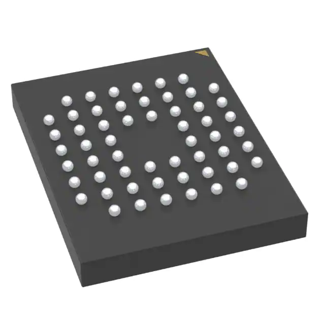
- Part No.:
- S29PL032J70BFA073
- Manufacturer:
- Infineon Technologies
- Category:
- Memory
- Package:
- 56-VFBGA
- Datasheet:
-
 S29PL032J70BFA073.pdf
- Description:
- IC FLASH 32MBIT PARALLEL 56FBGA
- Quantity:
- Payment:

- Shipping:

Inventory:1,909
Please send an inquiry. Send us your inquiry, and we will respond immediately.
Product details
Overview
S29PL032J70BFA073 from Infineon Technologies (formerly Cypress) is a 32-Mbit (2 M × 16-bit), 3.0 V-only Page Mode Flash memory with Simultaneous Read/Write capability across four independent banks, Enhanced VersatileI/O™ supporting 3 V I/O, and persistent/password sector protection. It delivers 55 ns random access time, 20 ns page access time, and operates across 2.7–3.6 V for embedded boot code storage in industrial controllers.
For engineers reviewing the S29PL032J70BFA073 datasheet, S29PL032J70BFA073 pinout, S29PL032J70BFA073 application, or S29PL032J70BFA073 equivalent, key selection criteria include bank-level concurrent read/write operation, zero-latency switching between modes, 48-ball FBGA (VBK048) package compatibility, and CFI-compliant host reconfiguration support.
Technical Context
This device implements FlexBank Architecture with four physically isolated banks (A–D), enabling true simultaneous read and program/erase operations - e.g., reading from Bank A while erasing Bank C. Each bank supports independent command execution and status monitoring via DQ6/DQ7 polling and RY/BY# signaling.
Enhanced VersatileI/O™ fixes all I/O and control pin voltage tolerance and output drive to the VIO pin level (3 V for PL032J), decoupling interface logic from core VCC. Sector protection combines persistent PPB locking, 64-bit password authentication, and hardware WP#/ACC input for factory-accelerated programming or sector lockdown at VCC.
Key Specifications
| Parameter | Value and Actual Design Meaning |
|---|---|
| Memory Density | 32 Mbit (2 Mwords × 16-bit data bus) |
| Supply Voltage Range | 2.7–3.6 V - enables direct integration into 3.3 V systems without level-shifting |
| Random Access Time | 55 ns - determines minimum instruction fetch latency in boot ROM applications |
| Page Access Time | 20 ns - accelerates burst reads of adjacent instructions or configuration data |
| Endurance | 1 million program/erase cycles per sector - supports field firmware updates over product lifetime |
| Data Retention | 20 years typical - ensures long-term reliability of stored boot code and calibration data |
| Standby Current | 0.2 µA typical - critical for low-power battery-backed systems during sleep mode |
Pinout & Package
Package: 8.15 mm × 6.15 mm, 48-ball Fine-pitch BGA (VBK048), RoHS-compliant, bottom-side thermal pad optional.
| Pin/Terminal | Circuit Role | Design Meaning |
|---|---|---|
| A0–A20 | Address Inputs | 21-bit address bus supporting full 2 Mword addressing; A0–A1 select byte within 16-bit word |
| DQ0–DQ15 | Data I/O | 16-bit bidirectional data bus; driven at VIO level (3 V) with ±10 mA drive strength |
| CE#, OE#, WE# | Chip/Output/Write Enable | Standard asynchronous control signals; active-low, TTL-compatible thresholds |
| RY/BY# | Ready/Busy Output | Open-drain status indicator - low during active program/erase, high when ready |
| RESET# | Hardware Reset Input | Asynchronous reset to reading state; pulls internal state machine to known initial condition |
| WP#/ACC | Write Protect/Acceleration | VIL = hardware lock on top/bottom 4K-word sectors; VIH = unlock; VHH = factory programming mode |
| VIO | I/O Supply Reference | Defines all I/O voltage levels - set to 3 V for PL032J; enables mixed-voltage system interfacing |
Key Features
| Feature | Design Value |
|---|---|
| FlexBank Architecture | Four independent banks (A–D) allow concurrent read + erase/program with zero latency switching |
| Enhanced VersatileI/O™ | VIO pin sets all I/O voltage levels - eliminates external level shifters in 3 V systems |
| CFI Compliance | Provides standardized JEDEC JESD68 register map for automatic host software reconfiguration |
| Password Sector Protection | 64-bit user-defined password required to unlock protected sectors - prevents unauthorized firmware modification |
| Erase/Program Suspend | Pause ongoing erase/program to service real-time read requests from other sectors - maintains system responsiveness |
Applications
| Industrial PLC Firmware Storage | Automotive ECU Boot Memory |
|---|---|
Use Scenario: Storing boot loader and safety-critical firmware in programmable logic controllers operating in harsh temperature environments. IC Role / Device Role / Timing Role: Non-volatile boot ROM with fast random access for instruction fetch and page-mode reads for parameter tables. Use Value: 55 ns access time reduces CPU wait states; 1M-cycle endurance supports field firmware patches over 10+ year deployment. | Use Scenario: Holding certified boot code and calibration data in engine control units requiring AEC-Q100 compliance. IC Role / Device Role / Timing Role: Secure, persistent storage with hardware write protection and password-locked sectors for ASIL-B functional safety. Use Value: WP#/ACC pin enables hardware lock of boot sectors; password protection prevents unauthorized reprogramming during diagnostics. |
| Medical Device Configuration Memory | Networking Equipment BIOS Storage |
Use Scenario: Retaining device-specific calibration coefficients and regulatory configuration profiles in portable diagnostic equipment. IC Role / Device Role / Timing Role: Low-power, long-retention nonvolatile memory accessed during power-up initialization and runtime parameter recall. Use Value: 0.2 µA standby current extends battery life; 20-year data retention meets FDA 510(k) archival requirements. | Use Scenario: Storing UEFI/BIOS images and hardware initialization routines in enterprise switches and routers. IC Role / Device Role / Timing Role: High-reliability flash with CFI interface for automatic firmware detection and update rollback support. Use Value: CFI compliance allows generic BIOS updater tools to auto-identify device geometry; simultaneous read/write enables background firmware validation. |
Equivalent & Alternatives
The following parts are listed as comparable options for similar Flash memory applications.
| Alternative Part | Technical Difference | Application Difference | Selection Advice |
|---|---|---|---|
| S29GL032N90TFIR20 | 48-ball BGA, 32 Mbit, 90 ns access, single-bank architecture, no simultaneous read/write | Lacks FlexBank concurrency; suitable only for simpler boot ROMs without background updates | Select when cost sensitivity outweighs need for concurrent operations and latency-critical performance |
| MX29GL320EHTI-90G | 48-ball BGA, 32 Mbit, 90 ns access, CFI-compliant, no password protection or VIO pin | No hardware sector lock or password security; lacks VersatileI/O flexibility for mixed-voltage designs | Choose where basic flash functionality suffices and security features are managed externally |
Compared with S29GL032N90TFIR20 and MX29GL320EHTI-90G, the S29PL032J70BFA073 uniquely delivers zero-latency bank concurrency, 3 V VersatileI/O, and dual-layer sector protection - making it optimal for real-time embedded systems requiring secure, updatable boot memory.
Availability
S29PL032J70BFA073 is available at Aetrix Electronics and suitable for industrial PLC firmware storage, automotive ECU boot memory, and medical device configuration memory requiring stable component supply, long-term lifecycle support, and RoHS-compliant packaging.
Supply support for S29PL032J70BFA073 includes scheduled delivery planning, volume procurement assistance, BOM continuity management, traceable sourcing, and lifecycle availability coordination for OEM customers, industrial embedded developers, connected-device designers, and electronics production programs.
Manufacturer
Infineon Technologies is a global semiconductor leader headquartered in Munich, Germany, specializing in power management, automotive, industrial, and security solutions.
The S29PL-J series was developed by Cypress (acquired by Infineon in 2020) to deliver high-reliability, multi-bank Flash memory for mission-critical embedded boot and firmware applications demanding concurrent access and robust security.
FAQ
Does S29PL032J70BFA073 support true simultaneous read and write operations?
Yes - its FlexBank Architecture divides memory into four independent banks (A–D), allowing one bank to be read while another executes erase or program operations with zero latency. This is confirmed in the datasheet's Section 2 and Table 1, which define bank sizes and concurrent operation capability for PL032J.
What is the function of the VIO pin on S29PL032J70BFA073?
The VIO pin sets the voltage reference for all I/O pins (DQ0–DQ15) and control inputs (CE#, OE#, WE#, etc.). For PL032J, VIO is fixed at 3 V, ensuring compatible interfacing with standard 3.3 V microcontrollers without external level shifters - detailed in Section 1.1 and "Enhanced VersatileI/O™" feature description.
How does sector protection work on this device?
Sector protection uses three methods: (1) Persistent PPB bits locked at VCC to permanently disable program/erase; (2) 64-bit password authentication for dynamic unlock; and (3) hardware WP# pin to lock top/bottom 4K-word sectors. All are documented in Sections 11–13 and supported by command sequences in Section 15.
Is CFI (Common Flash Interface) implemented in S29PL032J70BFA073?
Yes - the device fully complies with JEDEC JESD68 CFI specification, exposing standardized registers (Query, Primary, Alternate) that report geometry, timing, and command set details. This enables host software to auto-detect and configure the device, as verified in Section 14 and CFI query response tables.
S29PL032J70BFA073 Specifications
- Product attributes
- Attribute value
- Manufacturer:
- Infineon Technologies
- Series:
- PL-J
- Package/Case:
- 56-VFBGA
- Packaging:
- Tape & Reel (TR)
- Product Status:
- Active
- Programmable:
- Not Verified
- Memory Type:
- Non-Volatile
- Memory Format:
- FLASH
- Technology:
- FLASH - NOR
- Memory Size:
- 32Mbit
- Memory Organization:
- 2M x 16
- Memory Interface:
- Parallel
- Clock Frequency:
- -
- Write Cycle Time - Word, Page:
- 70ns
- Access Time:
- 70 ns
- Voltage - Supply:
- 2.7V ~ 3.6V
- Operating Temperature:
- -40°C ~ 85°C (TA)
- Grade:
- -
- Qualification:
- -
- Mounting Type:
- Surface Mount
- Supplier Device Package:
- 56-FBGA (9x7)
S29PL032J70BFA073 FAQ
1.How can I place an order for S29PL032J70BFA073 through Aetrix?
Please submit a Request for Quotation (RFQ) for S29PL032J70BFA073 on Aetrix. Our sales agent will provide a competitive quotation and guide you through the order confirmation once you accept the terms.
2.Are the price and stock information for S29PL032J70BFA073 reliable?
The price and inventory of S29PL032J70BFA073 are updated periodically and may fluctuate due to market conditions. Stock and pricing data are typically refreshed every 24 hours. Quotation validity for S29PL032J70BFA073 is usually 5 days.
3.What payment methods are accepted for S29PL032J70BFA073?
We accept Wire Transfer, PayPal, Credit Card, Western Union, MoneyGram, and Escrow for S29PL032J70BFA073 transactions.
Note: Certain payment methods may incur a processing fee.
4.How is shipping managed for S29PL032J70BFA073?
S29PL032J70BFA073 orders can be shipped via leading logistics carriers, including DHL, UPS, FedEx, TNT, or Registered Mail.
Once your S29PL032J70BFA073 order is processed, you will receive an email with the shipment details and tracking number.
Note: Tracking information may take up to 24 hours to appear. Express delivery typically takes 3–5 business days.
5.How can I obtain technical support or documentation for S29PL032J70BFA073?
For technical support, including S29PL032J70BFA073 datasheets, pinout diagrams, or application guidance, please contact our engineering support team. They can provide detailed documentation and assistance for your S29PL032J70BFA073 requirements.
6.How does Aetrix verify that S29PL032J70BFA073 is sourced from the original manufacturer or authorized distributors?
All S29PL032J70BFA073 products on Aetrix are procured from qualified distributors and authorized channels. Our dedicated quality assurance team conducts strict verification, including traceability checks and, if necessary, third-party testing. This ensures that S29PL032J70BFA073 meets industry standards.
7.What is the process for return or replacement of S29PL032J70BFA073?
All S29PL032J70BFA073 units undergo pre-shipment inspection (PSI). If there is an issue with S29PL032J70BFA073, returns or replacements are accepted under the following conditions:
1.Quantity discrepancies, incorrect items, or visible external defects (such as breakage or corrosion), acknowledged by Aetrix.
2.The issue is reported within 90 days of delivery.
3.The S29PL032J70BFA073 part is unused and in its original packaging.
Return procedure for S29PL032J70BFA073:
1.Submit a request within 90 days.
2.Obtain a Return Material Authorization (RMA) from Aetrix.
S29PL032J70BFA073 Tags

-
M24C02-WMN6TP
STMicroelectronics

-
AT24C02C-XHM-T
Microchip Technology

-
AT21CS01-STUM10-T
Microchip Technology

-
AT24C02C-SSHM-T
Microchip Technology

-
24LC01BT-I/OT
Microchip Technology

-
M24C02-FMC6TG
STMicroelectronics
-
AT24CS02-SSHM-T
Microchip Technology

-
93LC46BT-I/OT
Microchip Technology
-
AT24C04C-SSHM-T
Microchip Technology

-
24LC01BT-I/SN
Microchip Technology
-
24AA02UIDT-I/OT
Microchip Technology

-
AT24C08C-STUM-T
Microchip Technology
Tech Hub

A practical engineering guide to 3.3V and 5V logic compatibility, input thresholds, resistor dividers, translator ICs, MOSFET level shifting, I2C pull-ups, timing limits and power-sequencing risks.

The 74HC595 uses push-pull logic outputs, while the TPIC6B595 uses 50 V open-drain DMOS sinks for higher-power loads. This guide compares timing, current limits, 3.3 V interfacing, load wiring, thermal…

The 74HC595 converts serial data into eight stable parallel outputs. This guide covers pin functions, shift and storage timing, OE and MR behavior, drive-current limits, cascading, voltage compatibilit…

A technical comparison of level-sensitive latches and edge-triggered flip-flops, covering timing windows, setup and hold limits, master–slave operation, time borrowing, race-through, HDL inference and…

A D latch stores one bit while Enable controls when data can pass. This reference covers gate-level operation, truth tables, transparency, setup and hold timing, LE versus OE, common ICs and practical …

An SR latch stores one bit through cross-coupled feedback. This engineering reference covers NOR and NAND implementations, truth tables, forbidden-state recovery, gated operation, switch debouncing, fa…

Latch circuits retain one bit through feedback. This technical reference covers SR and D latches, truth tables, transparency, timing limits, latch-versus-flip-flop behavior, applications and common log…

An engineering guide to LED driver operation, constant-current and constant-voltage outputs, linear and switching topologies, dimming, IC selection, calculations, replacement compatibility, and fault c…

Operational amplifier guide covering op amp basics, feedback, ideal vs real op amps, common configurations, buffer circuits, offset, bias current, gain-bandwidth, slew rate, rail-to-rail limits and sel…

Jumper cables guide covering safe connection order, red and black clamp placement, final ground connection, cable gauge, length, clamp quality, copper vs CCA cables, jump starter comparison and battery…


