
 My Inquiry
 My Account


Infineon Technologies S40410081B1B2W000
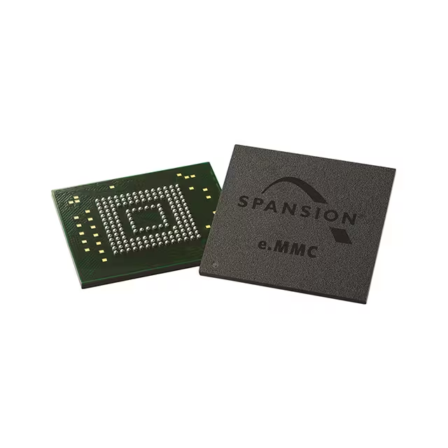
- Part No.:
- S40410081B1B2W000
- Manufacturer:
- Infineon Technologies
- Category:
- Memory
- Package:
- 100-LBGA
- Datasheet:
-
 S40410081B1B2W000.pdf
- Description:
- IC FLASH 8GBIT PARALLEL 100LBGA
- Quantity:
- Payment:

- Shipping:

Inventory:2,746
Please send an inquiry. Send us your inquiry, and we will respond immediately.
Product details
Overview
S40410081B1B2W000 from Cypress Semiconductor is an 8 GB e.MMC 4.51-compliant embedded flash memory device with integrated controller, operating at 2.7–3.6 V (VCC) and 1.7–1.95 V or 2.7–3.6 V (VCCQ), supporting HS200 mode up to 200 MHz, 120 MB/s sequential read, and 20 MB/s sequential write in x8 I/O configuration. It is used in industrial embedded systems requiring boot partitioning, RPMB security, and high-reliability storage.
For engineers reviewing the S40410081B1B2W000 datasheet, S40410081B1B2W000 pinout, S40410081B1B2W000 application, or S40410081B1B2W000 equivalent, key selection criteria include HS200 timing compliance, 153-ball VFBGA package dimensions (13 mm × 11.5 mm × 1.0 mm), boot partition support, RPMB authentication capability, and industrial temperature range (−40 °C to +85 °C).
Technical Context
The S40410081B1B2W000 implements JEDEC JESD84-B451 e.MMC 4.51 specification with full backward compatibility to earlier e.MMC versions. Its architecture integrates a dedicated MMC I/O block, NAND I/O block, and Cypress-optimized flash management firmware enabling wear-leveling, ECC, garbage collection, and defect management.
It supports three operational modes: SDR (up to 52 MHz), DDR (up to 52 MHz), and HS200 (up to 200 MHz), with configurable bus widths (1/4/8-bit in SDR; 4/8-bit in DDR/HS200). Boot operation is enabled via CMD0 with argument 0xFFFFFFFA, requiring ≤150 ms for boot partition access.
Key Specifications
| Parameter | Value and Actual Design Meaning |
|---|---|
| Density | 8 GB usable storage in MLC NAND with factory-configured 4 MB boot partitions and 4 MB RPMB partition |
| Interface Standard | e.MMC 4.51 (JESD84-B451), backward compatible with e.MMC 4.4/4.3 |
| Bus Speed Mode | HS200 mode enables 200 MHz clock with 8-bit data bus for 120 MB/s read throughput |
| Operating Voltage | VCC: 2.7–3.6 V (flash core); VCCQ: 1.7–1.95 V or 2.7–3.6 V (I/O interface) |
| Temperature Range | Industrial grade: −40 °C to +85 °C ambient operating temperature |
| Package | 153-ball Very Thin Fine-Pitch BGA (VFBGA), 13 mm × 11.5 mm × 1.0 mm, 0.5 mm ball pitch |
| Reliability Features | Replay Protected Memory Block (RPMB) with HMAC-SHA256 authentication and one-time programmable GP partition configuration |
Pinout & Package
Package: 153-ball VFBGA (13 mm × 11.5 mm × 1.0 mm, 0.5 mm pitch), balls-down orientation.
| Pin/Terminal | Circuit Role | Design Meaning |
|---|---|---|
| DAT0–DAT7 | Bidirectional data I/O | 8-bit parallel data bus supporting SDR/DDR/HS200 modes; requires controlled impedance routing |
| CMD | Bidirectional command I/O | Carries initialization commands (e.g., CMD0 boot trigger) and status responses; open-drain/push-pull configurable |
| CLK | Input clock | Master clock input up to 200 MHz in HS200; must meet setup/hold timing relative to DAT/CMD edges |
| RST_N | Active-low hardware reset | Asynchronous reset signal asserting internal state machine; requires ≥100 µs low pulse for full initialization |
| VCC / VCCQ / VSS / VSSQ / VDDI | Power and ground terminals | VCC powers NAND array; VCCQ powers I/O logic; VDDI is internal regulator node requiring 1 µF decoupling to VSS |
Key Features
| Feature | Design Value |
|---|---|
| HS200 Interface Support | Enables 200 MHz clock with 8-bit bus for 120 MB/s sequential read-critical for fast boot and firmware loading |
| Boot Partition Architecture | Two factory-configured 4 MB boot partitions in Enhanced (SLC) mode ensure deterministic boot latency and endurance |
| Replay Protected Memory Block (RPMB) | 4 MB authenticated storage using HMAC-SHA256; prevents replay attacks on secure keys and firmware signatures |
| Auto Background Operations | Garbage collection and wear-leveling execute during idle cycles without host intervention-reducing write amplification |
| One-Time Programmable GP Partitions | Host configures up to four General Purpose Partitions with fixed size and SLC/MLC mode-enabling mixed-reliability storage mapping |
Applications
| Industrial HMI Panel | Medical Diagnostic Imaging Device |
|---|---|
Use Scenario: Touchscreen-based human-machine interface running Linux OS with local firmware updates and calibration data logging. IC Role / Device Role / Timing Role: Primary boot and system storage device hosting kernel, rootfs, and secure RPMB-stored calibration certificates. Use Value: Industrial temperature rating (−40 °C to +85 °C) ensures reliability in uncontrolled environments; HS200 mode reduces boot time by >35% vs. SDR. | Use Scenario: Portable ultrasound unit requiring rapid image capture, DICOM export, and HIPAA-compliant audit log storage. IC Role / Device Role / Timing Role: Secure storage for encrypted patient images and digitally signed audit logs using RPMB partition. Use Value: RPMB authentication prevents tampering with medical records; 1400 IOPS random write supports concurrent image buffering and metadata logging. |
| Gaming Console Set-Top Box | Automotive Infotainment Head Unit |
Use Scenario: Streaming media box with local game cache, firmware OTA updates, and user profile persistence. IC Role / Device Role / Timing Role: High-throughput storage for 4K video decode buffers and background firmware validation. Use Value: 120 MB/s sequential read sustains sustained 4K playback; Trim command enables efficient space reclamation after app uninstallation. | Use Scenario: In-vehicle navigation system storing map tiles, voice recognition models, and over-the-air update packages. IC Role / Device Role / Timing Role: Dual-boot partitioning allows A/B firmware updates with zero downtime and rollback capability. Use Value: Factory-configured boot partitions enable atomic firmware swaps; Sanitize command erases sensitive location history before resale. |
Equivalent & Alternatives
The following parts are listed as comparable options for similar e.MMC storage applications.
| Alternative Part | Technical Difference | Application Difference | Selection Advice |
|---|---|---|---|
| SanDisk iNAND MC2128 (SDINBDG4-8) | Same 8 GB density and 153-ball VFBGA, but compliant with e.MMC 5.1; supports HS400 mode (up to 400 MHz) | Lacks RPMB partition; uses proprietary secure boot instead of JEDEC-standard RPMB authentication | Select when HS400 bandwidth is required and RPMB is not mandated by security policy |
| SK hynix H9TP32A8JDACPR-NEE | 8 GB e.MMC 4.51 device in 153-ball VFBGA; identical voltage and temperature specs but lower 100 MB/s sequential read (vs. 120 MB/s) | Supports same boot/RPMB features but with reduced random write IOPS (1200 vs. 1400) | Select when cost sensitivity outweighs marginal performance loss in non-latency-critical applications |
Compared with SanDisk iNAND MC2128 and SK hynix H9TP32A8JDACPR-NEE, the S40410081B1B2W000 delivers higher sequential read throughput (120 MB/s) and certified RPMB implementation per JEDEC JESD84-B451, making it preferred for security-audited industrial and medical deployments where standardized cryptographic storage is required.
Availability
S40410081B1B2W000 is available at Aetrix Electronics and suitable for industrial HMI panels, medical diagnostic imaging devices, and automotive infotainment head units requiring stable component supply, long-term lifecycle support, and JEDEC-compliant secure storage.
Supply support for S40410081B1B2W000 includes scheduled delivery planning, volume procurement assistance, BOM continuity management, traceable sourcing, and lifecycle availability coordination for OEM customers, industrial embedded developers, connected-device designers, and electronics production programs.
Manufacturer
Cypress Semiconductor (now part of Infineon Technologies) is a fabless semiconductor company specializing in embedded systems solutions, including microcontrollers, connectivity, memory, and analog ICs.
The S40410081B1B2W000 belongs to Cypress's e.MMC product line, designed specifically for embedded applications demanding high reliability, industrial temperature operation, and JEDEC-standard security features like RPMB and boot partitioning.
FAQ
What is the maximum supported clock frequency in HS200 mode?
The S40410081B1B2W000 supports up to 200 MHz in HS200 mode when configured with an 8-bit data bus. This is specified in the AC timing section of the official datasheet (Document Number 002-02760 Rev. *H, Page 20), and requires precise PCB layout with matched trace lengths and proper termination to meet setup/hold margins.
Does this device support hardware reset with guaranteed initialization behavior?
Yes. The RST_N pin provides asynchronous hardware reset functionality. A low pulse ≥100 µs initiates full internal state machine reset and reinitialization, including register reload and NAND array verification. This behavior is defined in Section 8 (Hardware Reset) of the datasheet and is independent of power sequencing.
Can the RPMB partition be used without host-side cryptographic libraries?
No. RPMB operation requires host-side implementation of HMAC-SHA256 and key programming via CMD23/25/26. The device performs only the cryptographic verification; the host must generate and manage the shared key, nonce, and message authentication code per JEDEC JESD84-B451 Section 6.7. Cypress provides reference firmware examples but no on-die crypto acceleration.
Is the 153-ball VFBGA package lead-free and RoHS compliant?
Yes. The S40410081B1B2W000 uses a lead-free, RoHS-compliant 153-ball VFBGA package with matte tin surface finish. Compliance is documented in Cypress's "Environmental Compliance Report" (ECR-001274), which confirms exemption 7a for lead in ceramic packages and full adherence to EU RoHS Directive 2011/65/EU Annex II.
S40410081B1B2W000 Specifications
- Product attributes
- Attribute value
- Manufacturer:
- Infineon Technologies
- Series:
- e.MMC 1B1
- Package/Case:
- 100-LBGA
- Packaging:
- Tray
- Product Status:
- Obsolete
- Programmable:
- Not Verified
- Memory Type:
- Non-Volatile
- Memory Format:
- FLASH
- Technology:
- FLASH - NAND
- Memory Size:
- 8Gbit
- Memory Organization:
- 1G x 8
- Memory Interface:
- Parallel
- Clock Frequency:
- 200 MHz
- Write Cycle Time - Word, Page:
- -
- Access Time:
- -
- Voltage - Supply:
- 2.7V ~ 3.6V
- Operating Temperature:
- -25°C ~ 85°C (TA)
- Grade:
- -
- Qualification:
- -
- Mounting Type:
- Surface Mount
- Supplier Device Package:
- 100-LBGA (14x18)
S40410081B1B2W000 FAQ
1.How can I place an order for S40410081B1B2W000 through Aetrix?
Please submit a Request for Quotation (RFQ) for S40410081B1B2W000 on Aetrix. Our sales agent will provide a competitive quotation and guide you through the order confirmation once you accept the terms.
2.Are the price and stock information for S40410081B1B2W000 reliable?
The price and inventory of S40410081B1B2W000 are updated periodically and may fluctuate due to market conditions. Stock and pricing data are typically refreshed every 24 hours. Quotation validity for S40410081B1B2W000 is usually 5 days.
3.What payment methods are accepted for S40410081B1B2W000?
We accept Wire Transfer, PayPal, Credit Card, Western Union, MoneyGram, and Escrow for S40410081B1B2W000 transactions.
Note: Certain payment methods may incur a processing fee.
4.How is shipping managed for S40410081B1B2W000?
S40410081B1B2W000 orders can be shipped via leading logistics carriers, including DHL, UPS, FedEx, TNT, or Registered Mail.
Once your S40410081B1B2W000 order is processed, you will receive an email with the shipment details and tracking number.
Note: Tracking information may take up to 24 hours to appear. Express delivery typically takes 3–5 business days.
5.How can I obtain technical support or documentation for S40410081B1B2W000?
For technical support, including S40410081B1B2W000 datasheets, pinout diagrams, or application guidance, please contact our engineering support team. They can provide detailed documentation and assistance for your S40410081B1B2W000 requirements.
6.How does Aetrix verify that S40410081B1B2W000 is sourced from the original manufacturer or authorized distributors?
All S40410081B1B2W000 products on Aetrix are procured from qualified distributors and authorized channels. Our dedicated quality assurance team conducts strict verification, including traceability checks and, if necessary, third-party testing. This ensures that S40410081B1B2W000 meets industry standards.
7.What is the process for return or replacement of S40410081B1B2W000?
All S40410081B1B2W000 units undergo pre-shipment inspection (PSI). If there is an issue with S40410081B1B2W000, returns or replacements are accepted under the following conditions:
1.Quantity discrepancies, incorrect items, or visible external defects (such as breakage or corrosion), acknowledged by Aetrix.
2.The issue is reported within 90 days of delivery.
3.The S40410081B1B2W000 part is unused and in its original packaging.
Return procedure for S40410081B1B2W000:
1.Submit a request within 90 days.
2.Obtain a Return Material Authorization (RMA) from Aetrix.
S40410081B1B2W000 Tags

-
M24C02-WMN6TP
STMicroelectronics

-
AT24C02C-XHM-T
Microchip Technology

-
AT21CS01-STUM10-T
Microchip Technology

-
AT24C02C-SSHM-T
Microchip Technology

-
24LC01BT-I/OT
Microchip Technology

-
M24C02-FMC6TG
STMicroelectronics
-
AT24CS02-SSHM-T
Microchip Technology

-
93LC46BT-I/OT
Microchip Technology
-
AT24C04C-SSHM-T
Microchip Technology

-
24LC01BT-I/SN
Microchip Technology
-
24AA02UIDT-I/OT
Microchip Technology

-
AT24C08C-STUM-T
Microchip Technology
Tech Hub

Latch circuits retain one bit through feedback. This technical reference covers SR and D latches, truth tables, transparency, timing limits, latch-versus-flip-flop behavior, applications and common log…

An engineering guide to LED driver operation, constant-current and constant-voltage outputs, linear and switching topologies, dimming, IC selection, calculations, replacement compatibility, and fault c…

Operational amplifier guide covering op amp basics, feedback, ideal vs real op amps, common configurations, buffer circuits, offset, bias current, gain-bandwidth, slew rate, rail-to-rail limits and sel…

Jumper cables guide covering safe connection order, red and black clamp placement, final ground connection, cable gauge, length, clamp quality, copper vs CCA cables, jump starter comparison and battery…

LDO regulator guide covering low dropout voltage, power dissipation, thermal design, PSRR, output noise, capacitor stability, adjustable LDO circuits, LDO vs buck converter and datasheet selection chec…

Conditional Access Module guide covering CAM meaning, CI/CI+ interface, smart card authorization, DVB security workflow, TV and set-top box compatibility, internal electronics, ESD protection, connecto…

Guide to electronic component obsolescence covering EOL risk, PCN/PDN notices, last-time buy planning, replacement options, form-fit-function validation, counterfeit risk and BOM lifecycle management.

18650 battery guide covering lithium-ion cell basics, 3.6V/3.7V voltage, 4.2V charging, mAh and Wh capacity, protected cells, chargers, BMS, series-parallel packs, holders, welding and sourcing checks.…

Hall effect sensor guide covering working principle, linear and digital sensors, Arduino circuits, current sensing, speed detection, automotive applications, A3144 examples, signal filtering and datash…

Product Change Notification guide for electronic components, covering PCN meaning, PCN vs PDN/EOL, common change types, risk levels, form-fit-function review, engineering validation, BOM control, LTB/L…


