
 My Inquiry
 My Account


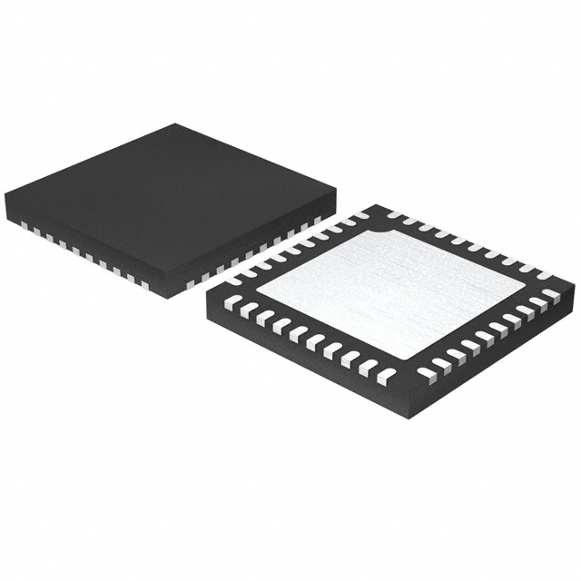
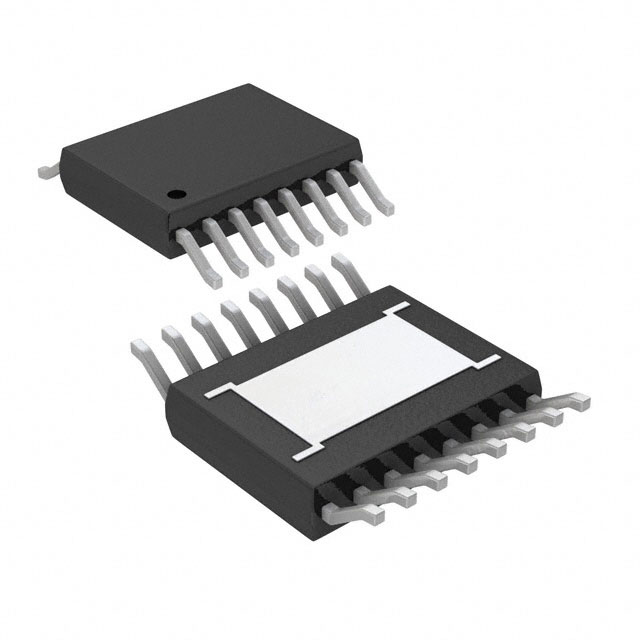
Infineon Technologies S6BP401AY1SN1B000
- Part No.:
- S6BP401AY1SN1B000
- Manufacturer:
- Infineon Technologies
- Category:
- Voltage Regulators - Linear + Switching
- Package:
- 40-VFQFN Exposed Pad
- Datasheet:
-
 S6BP401AY1SN1B000.pdf
- Description:
- IC REG 6OUT BUCK/LNR SYNC 40QFN
- Quantity:
- Payment:

- Shipping:

Inventory:1,385
Please send an inquiry. Send us your inquiry, and we will respond immediately.
Product details
Overview
S6BP401AY1SN1B000 from Infineon Technologies (formerly Cypress) is an AEC-Q100 Grade-1 automotive power management IC for ADAS platforms, integrating quad 2.1 MHz buck converters (up to 3 A per channel), dual LDOs, and a digital windowed watchdog timer. It operates from 4.5–5.5 V input, delivers preset output voltages including 1.20–1.575 V/2 A (DD1), 1.00–1.275 V/3 A (DD2), 1.20–2.575 V/2 A (DD3), and 3.3–3.4 V/1 A (DD4), and supports camera system power sequencing.
For engineers reviewing the S6BP401AY1SN1B000 datasheet, S6BP401AY1SN1B000 pinout, S6BP401AY1SN1B000 application, or S6BP401AY1SN1B000 equivalent, key selection criteria include its integrated FETs enabling 2.4 MHz switching, load-independent soft-start, independent enable control per rail, power-good monitoring per regulator, and thermal/overcurrent/overvoltage protection in a 6 mm × 6 mm QFN-40 package.
Technical Context
The S6BP401AY1SN1B000 employs current-mode control architecture across all four buck channels, delivering fast transient response and stable regulation under dynamic load conditions. Each buck converter integrates high-side and low-side MOSFETs rated for up to 3 A continuous output current and supports both internal (2.0–2.2 MHz) and external clock synchronization (1.8–2.4 MHz).
The dual LDOs accept 2.97–5.5 V input and provide fixed or resistor-programmable outputs with built-in voltage-setting resistors; the integrated windowed watchdog timer features WDI trigger input and RST reset output with configurable timeout windows, and all regulators include independent enable pins, power-good flags, and discharge resistors.
Key Specifications
| Parameter | Value and Actual Design Meaning |
|---|---|
| Input Voltage Range | 4.5 V to 5.5 V for buck converters; 2.97 V to 5.5 V for LDOs - supports direct connection to automotive 5 V rail with margin for transients. |
| Switching Frequency | 2.1 MHz nominal (2.0–2.2 MHz internal / 1.8–2.4 MHz external sync) - enables compact magnetics and reduces EMI in high-density ADAS PCB layouts. |
| Max Output Current | 3 A (DD2), 2 A (DD1 & DD3), 1 A (DD4), 0.2 A (LD2), 0.5 A (LD1) - matches sensor, SoC core, I/O, and interface rail requirements in camera ECU designs. |
| Output Voltage Accuracy | ±1.5% over temperature and line/load - ensures reliable operation of sensitive image signal processors and SerDes interfaces. |
| UVLO Threshold | 4.25 V (typical) with hysteresis - prevents erratic startup during cold-crank or battery dip events in automotive environments. |
| Thermal Shutdown | 150 °C (typical) with automatic recovery - protects against sustained overload or poor heatsinking in sealed ADAS enclosures. |
| Package | 6 mm × 6 mm QFN-40 with exposed pad - provides low thermal resistance (θJA = 32 °C/W) and robust mechanical attachment for vibration-prone automotive mounting. |
Pinout & Package
Package: 6 mm × 6 mm, 40-pin QFN with exposed thermal pad (EP) and four corner pads (CP1–CP4), RoHS-compliant, AEC-Q100 Grade-1 qualified.
| Pin/Terminal | Circuit Role | Design Meaning |
|---|---|---|
| EN1–EN4, ENL1–ENL2 | Independent enable inputs | Allow precise power-up/down sequencing of each rail without external logic or timing components. |
| FB1–FB4 | Buck feedback inputs | Accept resistor-divider networks for custom output voltages; internal resistors enable preset outputs without external components. |
| PG1–PG4, PGL2 | Power-good open-drain outputs | Signal valid regulation status per rail; can drive MCU GPIOs or cascade into downstream enable chains. |
| LX1–LX4 | Switch-node outputs | Connect directly to external inductors; require careful layout to minimize EMI and switching losses. |
| VCC, PVCC1–PVCC4, PVCCL1–PVCCL2 | Supply inputs | Dedicated power domains isolate analog controller (VCC), buck drivers (PVCCx), and LDO inputs (PVCCLx) for noise immunity. |
| WDI, RST | Watchdog interface | WDI accepts pulse train to prevent timeout; RST asserts active-low reset on window violation - no external timer IC needed. |
Key Features
| Feature | Design Value |
|---|---|
| Integrated high-side/low-side FETs | Eliminates 8 external MOSFETs and gate drivers, reducing BOM count and board area by >30% vs discrete solutions. |
| Load-independent soft-start | Ensures monotonic voltage ramp regardless of output capacitance or load, preventing inrush-induced supply droop in multi-rail systems. |
| Built-in compensation circuits | Removes need for external Type-II/III compensation networks, simplifying design validation and reducing layout sensitivity. |
| Digital windowed watchdog timer | Provides fail-safe reset generation with programmable window width - critical for ASIL-B compliant camera domain controllers. |
| Independent power-good monitoring | Enables hierarchical power sequencing and fault isolation: each PG flag can trigger independent system-level diagnostics. |
Applications
| ADAS Camera ECU | Automotive Radar Processing Unit |
|---|---|
Use Scenario: Powering image sensor, ISP, and MIPI interface in front-facing monocular camera module. IC Role / Device Role / Timing Role: Primary PMIC managing six regulated rails: 1.2 V core, 1.8 V I/O, 2.8 V sensor bias, 3.3 V SerDes, 1.2 V analog, and 1.8 V reference. Use Value: Integrated sequencing, PG monitoring, and watchdog eliminate need for external supervisors and reduce startup time to <100 ms. | Use Scenario: Supplying RF transceiver, DSP, memory, and CAN FD interface in 77 GHz radar ECU. IC Role / Device Role / Timing Role: Central power hub delivering 1.0 V DSP core, 1.2 V memory I/O, 1.8 V ADC reference, 3.3 V CAN transceiver, and two LDO-sourced analog supplies. Use Value: AEC-Q100 Grade-1 rating and thermal shutdown ensure reliability at junction temperatures up to 125 °C ambient. |
| Driver Monitoring System | In-Cabin Occupancy Sensor Hub |
Use Scenario: Powering IR LED driver, ToF sensor, and vision processor in driver drowsiness detection module. IC Role / Device Role / Timing Role: Supplies 1.2 V processor core, 1.8 V image pipeline, 2.5 V LED driver bias, 3.3 V communication interface, and two low-noise LDOs for analog sensing. Use Value: Independent enable control allows dynamic rail shutdown during sleep mode, cutting quiescent current to <50 µA. | Use Scenario: Supporting multi-modal occupancy detection using mmWave, thermal, and capacitive sensors in center console. IC Role / Device Role / Timing Role: Delivers 1.2 V mmWave SoC core, 1.8 V RF front-end, 3.3 V sensor interface, 2.8 V thermal sensor bias, and dual LDOs for precision analog references. Use Value: Built-in discharge resistors ensure rapid rail collapse during power-off, meeting ISO 16750-2 transient immunity requirements. |
Equivalent & Alternatives
The following parts are listed as comparable options for similar automotive PMIC applications.
| Alternative Part | Technical Difference | Application Difference | Selection Advice |
|---|---|---|---|
| MPQ4436-AEC1 | Single 3.5 A buck with external FETs; no integrated LDOs or watchdog; 2.2 MHz switching. | Requires external LDOs, supervisor, and sequencing logic - increases BOM and layout complexity. | Select when only one high-current rail is needed and system-level supervision already exists. |
| TPS65381A-Q1 | Triple buck + dual LDO + watchdog; 1.2 MHz max frequency; 2.5 A max per buck; larger 7 mm × 7 mm HTSSOP-48 package. | Lower switching frequency demands larger inductors; higher pin count complicates routing in space-constrained camera modules. | Select when lower EMI priority outweighs size constraints and 2.1 MHz operation is not required. |
Compared with MPQ4436-AEC1 and TPS65381A-Q1, the S6BP401AY1SN1B000 uniquely combines quad buck capability, dual LDOs, and watchdog in a compact QFN-40 package with 2.1 MHz operation - optimizing board area, component count, and startup timing for ADAS camera ECUs.
Availability
S6BP401AY1SN1B000 is available at Aetrix Electronics and suitable for automotive ADAS camera modules, radar processing units, and driver monitoring systems requiring stable component supply, AEC-Q100 compliance, and long-term lifecycle support.
Supply support for S6BP401AY1SN1B000 includes scheduled delivery planning, volume procurement assistance, BOM continuity management, traceable sourcing, and lifecycle availability coordination for OEM customers, industrial embedded developers, connected-device designers, and electronics production programs.
Manufacturer
Infineon Technologies is a global semiconductor leader focused on power systems, automotive electronics, and security solutions, with deep expertise in high-reliability analog and mixed-signal ICs.
The S6BP401AY1SN1B000 belongs to Infineon's automotive PMIC portfolio designed specifically for advanced driver assistance systems, emphasizing integration, functional safety, and AEC-Q100 Grade-1 robustness in harsh automotive environments.
FAQ
What is the maximum allowable input voltage for the S6BP401AY1SN1B000 buck converters?
The absolute maximum input voltage for the buck converters (PVCC1–PVCC4) is 6.0 V, but the recommended operating range is 4.5 V to 5.5 V. Operation above 5.5 V risks violating the 6.0 V absolute maximum rating and may trigger overvoltage protection or cause permanent damage. Automotive battery transients must be clamped externally if exceeding this limit.
Can the S6BP401AY1SN1B000 operate without external feedback resistors?
Yes - the device includes internal resistor dividers enabling preset output voltages (e.g., 1.20 V, 1.80 V, 3.30 V) without external components. External resistors are only required when custom output voltages outside the factory-preset ranges are needed, and the FB pins must be properly terminated in either configuration.
How does the windowed watchdog timer function without external components?
The watchdog uses an internal oscillator and digital logic to monitor pulse intervals on the WDI pin. If pulses fall outside the programmed window (e.g., too early or too late), RST asserts low. No external RC network or crystal is required - timing is set via internal registers accessible through I²C or hardware strapping options defined in the datasheet.
Is the exposed pad (EP) electrically connected to ground internally?
Yes - the exposed pad is internally connected to the GND net and must be soldered to a solid PCB ground plane for thermal dissipation and electrical stability. Thermal resistance drops from 65 °C/W (no pad connection) to 32 °C/W (fully connected), and floating the pad violates AEC-Q100 thermal test requirements.
S6BP401AY1SN1B000 Specifications
- Product attributes
- Attribute value
- Manufacturer:
- Infineon Technologies
- Series:
- -
- Package/Case:
- 40-VFQFN Exposed Pad
- Packaging:
- Tape & Reel (TR)
- Product Status:
- Active
- Topology:
- Step-Down (Buck) Synchronous (4), Linear (LDO) (2)
- Number of Outputs:
- 6
- Frequency - Switching:
- 2.1MHz
- Voltage/Current - Output 1:
- 1.5V, 2A
- Voltage/Current - Output 2:
- 1.1V, 3A
- Voltage/Current - Output 3:
- 2.5V, 2A
- w/LED Driver:
- No
- w/Supervisor:
- No
- w/Sequencer:
- No
- Voltage - Supply:
- 2.97V ~ 5.5V
- Operating Temperature:
- -40°C ~ 125°C (TA)
- Grade:
- Automotive
- Qualification:
- AEC-Q100
- Mounting Type:
- Surface Mount
- Supplier Device Package:
- 40-QFN (6x6)
S6BP401AY1SN1B000 FAQ
1.How can I place an order for S6BP401AY1SN1B000 through Aetrix?
Please submit a Request for Quotation (RFQ) for S6BP401AY1SN1B000 on Aetrix. Our sales agent will provide a competitive quotation and guide you through the order confirmation once you accept the terms.
2.Are the price and stock information for S6BP401AY1SN1B000 reliable?
The price and inventory of S6BP401AY1SN1B000 are updated periodically and may fluctuate due to market conditions. Stock and pricing data are typically refreshed every 24 hours. Quotation validity for S6BP401AY1SN1B000 is usually 5 days.
3.What payment methods are accepted for S6BP401AY1SN1B000?
We accept Wire Transfer, PayPal, Credit Card, Western Union, MoneyGram, and Escrow for S6BP401AY1SN1B000 transactions.
Note: Certain payment methods may incur a processing fee.
4.How is shipping managed for S6BP401AY1SN1B000?
S6BP401AY1SN1B000 orders can be shipped via leading logistics carriers, including DHL, UPS, FedEx, TNT, or Registered Mail.
Once your S6BP401AY1SN1B000 order is processed, you will receive an email with the shipment details and tracking number.
Note: Tracking information may take up to 24 hours to appear. Express delivery typically takes 3–5 business days.
5.How can I obtain technical support or documentation for S6BP401AY1SN1B000?
For technical support, including S6BP401AY1SN1B000 datasheets, pinout diagrams, or application guidance, please contact our engineering support team. They can provide detailed documentation and assistance for your S6BP401AY1SN1B000 requirements.
6.How does Aetrix verify that S6BP401AY1SN1B000 is sourced from the original manufacturer or authorized distributors?
All S6BP401AY1SN1B000 products on Aetrix are procured from qualified distributors and authorized channels. Our dedicated quality assurance team conducts strict verification, including traceability checks and, if necessary, third-party testing. This ensures that S6BP401AY1SN1B000 meets industry standards.
7.What is the process for return or replacement of S6BP401AY1SN1B000?
All S6BP401AY1SN1B000 units undergo pre-shipment inspection (PSI). If there is an issue with S6BP401AY1SN1B000, returns or replacements are accepted under the following conditions:
1.Quantity discrepancies, incorrect items, or visible external defects (such as breakage or corrosion), acknowledged by Aetrix.
2.The issue is reported within 90 days of delivery.
3.The S6BP401AY1SN1B000 part is unused and in its original packaging.
Return procedure for S6BP401AY1SN1B000:
1.Submit a request within 90 days.
2.Obtain a Return Material Authorization (RMA) from Aetrix.
S6BP401AY1SN1B000 Tags

-
TPS6521905RHBR
Texas Instruments
-
MIC3385YHL-TR
Microchip Technology
-
A4402ELPTR-T
Allegro MicroSystems

-
LM26480SQ-AA/NOPB
Texas Instruments
-
A4402KLPTR-T
Allegro MicroSystems
-
BD71847AMWV-E2
ROHM Semiconductor
-
ADP5040ACPZ-1-R7
Analog Devices Inc.
-
LT3048IDC#TRPBF
Analog Devices Inc.
-
ADP5037ACPZ-R7
Analog Devices Inc.

-
XRP7714ILB-F
MaxLinear, Inc.
-
LTC3260EDE#TRPBF
Analog Devices Inc.
-
LTC3260EMSE#PBF
Analog Devices Inc.
Tech Hub

Operational amplifier guide covering op amp basics, feedback, ideal vs real op amps, common configurations, buffer circuits, offset, bias current, gain-bandwidth, slew rate, rail-to-rail limits and sel…

Jumper cables guide covering safe connection order, red and black clamp placement, final ground connection, cable gauge, length, clamp quality, copper vs CCA cables, jump starter comparison and battery…

LDO regulator guide covering low dropout voltage, power dissipation, thermal design, PSRR, output noise, capacitor stability, adjustable LDO circuits, LDO vs buck converter and datasheet selection chec…

Conditional Access Module guide covering CAM meaning, CI/CI+ interface, smart card authorization, DVB security workflow, TV and set-top box compatibility, internal electronics, ESD protection, connecto…

Guide to electronic component obsolescence covering EOL risk, PCN/PDN notices, last-time buy planning, replacement options, form-fit-function validation, counterfeit risk and BOM lifecycle management.

18650 battery guide covering lithium-ion cell basics, 3.6V/3.7V voltage, 4.2V charging, mAh and Wh capacity, protected cells, chargers, BMS, series-parallel packs, holders, welding and sourcing checks.…

Hall effect sensor guide covering working principle, linear and digital sensors, Arduino circuits, current sensing, speed detection, automotive applications, A3144 examples, signal filtering and datash…

Product Change Notification guide for electronic components, covering PCN meaning, PCN vs PDN/EOL, common change types, risk levels, form-fit-function review, engineering validation, BOM control, LTB/L…

A practical guide to blend door actuators, covering HVAC function, symptoms, location, AC and heater issues, reset and calibration, replacement cost, electrical diagnosis, compatibility checks, and rep…

Engineering guide to Raspberry Pi alternatives, covering chip-level differences, Orange Pi, ROCK, Jetson, Banana Pi, NanoPi, Compute Module, Pico, GPIO, camera, HAT compatibility, and replacement risks…


