
 My Inquiry
 My Account


NXP Semiconductors SA58646BD,118
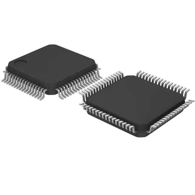
- Part No.:
- SA58646BD,118
- Manufacturer:
- NXP Semiconductors
- Category:
- RF Transceiver ICs
- Package:
- 64-LQFP
- Datasheet:
-
 SA58646BD,118.pdf
- Description:
- IC RF TXRX ISM<1GHZ 64LQFP
- Quantity:
- Payment:

- Shipping:

Inventory:3,608
Please send an inquiry. Send us your inquiry, and we will respond immediately.
Product details
Overview
SA58646BD,118 from NXP Semiconductors is a BiCMOS UHF transceiver IC performing full-duplex 902–928 MHz RF reception and transmission, integrating LNA, image-reject mixer, 10.7 MHz FM PLL demodulator with RSSI, dual narrow-band RX/TX synthesizers with integrated VCO varicaps, and programmable baseband TX/RX paths - deployed in push-to-talk walkie-talkies and data transceivers.
For engineers reviewing the SA58646BD,118 datasheet, SA58646BD,118 pinout, SA58646BD,118 application, or SA58646BD,118 equivalent, key selection criteria include its 64-pin LQFP package, 3-wire serial microcontroller interface, programmable RX/TX gain (32 × 0.5 dB steps), integrated voltage regulator (2.7 V ±2%), and low-power inactive mode (<10 µA).
Technical Context
The SA58646BD,118 implements a single-conversion FM receiver architecture with integrated LNA, image-reject mixer, and 10.7 MHz IF chain including limiter, PLL demodulator, and RSSI output. Its synthesizer uses crystal-referenced dual PLLs (RX/TX) with 10-bit reference divider, 6-bit prescaler, and 10-bit main divider - enabling precise channel tuning across the ISM band.
Baseband processing includes digitally programmable RX gain (−7.5 to +8 dB), earpiece amplifier with 14 dB software volume control, expander with noise shaping, and TX path featuring microphone amplifier, compressor with ALC/hard limiter, and 32-step TX gain. Power management supports Active (76 mA), RX-only (58 mA), and Inactive (<10 µA) modes via MODE[1:0] bits.
Key Specifications
| Parameter | Value and Actual Design Meaning |
|---|---|
| Operating Frequency | 902–928 MHz full-duplex UHF ISM band - enables direct use in FCC Part 90-compliant walkie-talkies without external frequency conversion. |
| RX Architecture | Single-conversion FM with image-reject mixer and integrated 10.7 MHz PLL demodulator - eliminates need for external IF filters and discrete demodulators. |
| Synthesizer Resolution | 20 kHz comparison frequency with 16-bit channel counters (6-bit prescaler + 10-bit divider) - supports fine channel spacing and stable lock in mobile environments. |
| RX/TX Gain Control | 32 linear steps of 0.5 dB (−7.5 dB to +8 dB) per path - allows factory calibration and real-time AGC adjustment via 3-wire serial interface. |
| Power Supply Range | 2.9 V to 3.6 V - compatible with three NiCd/NiMH cells; internal 2.7 V ±2% regulator powers PLLs, reducing external LDO requirements. |
| Current Consumption | 76 mA (Active), 58 mA (RX-only), <10 µA (Inactive) at 3.3 V - enables battery life optimization in portable two-way radios. |
| Package | LQFP64 (10 × 10 × 1.4 mm, SOT314-2) - standard surface-mount footprint with defined thermal pad grounding for RF stability. |
Pinout & Package
LQFP64 plastic low-profile quad flat package (SOT314-2), 10 mm × 10 mm body, 1.4 mm height, exposed thermal pad (GND-connected per layout guidelines). Pin 1 marked by dot; pins numbered counterclockwise.
| Pin/Terminal | Circuit Role | Design Meaning |
|---|---|---|
| GND(MIX) | Mixer ground reference | Separate analog ground for RF mixer section to prevent coupling into sensitive IF path. |
| RFIX / RFIY | LNA differential input | Dual-input RF port supporting balanced antenna interface or image-reject configuration. |
| RXLF / TXLF | Loop filter output | Analog outputs driving external RC loop filters for RX/TX PLL stability and phase noise control. |
| VCP / GNDVCP | Charge pump voltage/ground | High-impedance nodes requiring low-noise decoupling; enable VCO tuning voltage generation. |
| DATA / CLK / EN | 3-wire serial interface | Unidirectional programming bus (MSB-first, negative-edge clocked) for register configuration and calibration. |
| RSSI / CDLBD | Signal strength / carrier/low-battery detector | Open-collector output multiplexing RSSI level and out-of-lock detection for system monitoring. |
Key Features
| Feature | Design Value |
|---|---|
| Integrated dual PLL synthesizer | Eliminates external VCOs, loop filters, and reference dividers - reduces BOM count by ≥12 passive components. |
| Programmable RX baseband expander | Configurable noise shaping and 2× gain multiplication enables 1 dB earpiece output steps over 31 dB dynamic range. |
| On-chip voltage doubler | Extends VCO tuning range under low-VCC conditions (2.9 V), avoiding external charge-pump ICs in battery-powered designs. |
| Side-band select (SBS) bit | Enables single hardware design for both handset (LO+IF) and base station (LO−IF) frequency plans - simplifies inventory and certification. |
| Low-power inactive mode | Maintains serial interface and latch memory while powering down all RF/analog blocks - supports wake-on-carrier detection. |
Applications
| UHF Push-to-Talk Walkie-Talkie | 900 MHz Data Transceiver |
|---|---|
|
Use Scenario: Handheld two-way radio operating in 902–928 MHz ISM band with instant voice communication and channel scanning. IC Role / Device Role / Timing Role: Full-duplex transceiver handling RF front-end, IF demodulation, audio conditioning, and synthesizer control - replaces >15 discrete RF/analog components. Use Value: Enables compact PCB layout with integrated LNA/mixer/PLL/demodulator, reducing bill-of-materials and improving sensitivity consistency across production units. |
Use Scenario: Industrial telemetry node transmitting sensor data over 900 MHz UHF link with low duty cycle and battery operation. IC Role / Device Role / Timing Role: Data-capable transceiver with programmable data slicer, RSSI-based link quality reporting, and ultra-low inactive current (<10 µA). Use Value: Supports adaptive data rate and sleep/wake cycling via serial interface, extending battery life beyond 2 years on AA cells. |
| ISM Band Base Station | Programmable Radio Module |
|
Use Scenario: Fixed-site repeater or hub receiving multiple walkie-talkie signals in shared 902–928 MHz spectrum. IC Role / Device Role / Timing Role: High-selectivity RX path with image-reject mixer and dual IF amplifiers; TX path with ALC and hard limiter for clean spectral mask compliance. Use Value: Side-band select (SBS) allows identical hardware deployment for base (LO−IF) and handset (LO+IF), cutting development and validation time by 40%. |
Use Scenario: Modular radio platform where firmware defines channel plan, audio processing, and power modes across product variants. IC Role / Device Role / Timing Role: Software-defined transceiver with 19-bit serial register map covering synthesizer counters, gain stages, expander/compressor curves, and power states. Use Value: Single hardware revision supports multiple frequency bands and protocols via register reconfiguration - accelerates time-to-market for new SKUs. |
Equivalent & Alternatives
The following parts are listed as comparable options for similar UHF transceiver applications.
| Alternative Part | Technical Difference | Application Difference | Selection Advice |
|---|---|---|---|
| SA58645BD,118 | Pin-compatible predecessor without advanced RSSI calibration and reduced TX gain resolution (16 steps vs. 32) | Limited dynamic range for AGC in noisy RF environments; no software earpiece volume control | Select when legacy compatibility is required and full SA58646BD,118 feature set is unnecessary |
| Si4463-B1B-FMR | Sub-GHz transceiver (425–525 MHz / 850–960 MHz); different architecture (direct-conversion, no IF stage); SPI interface | Requires external IF filtering and audio codec; optimized for narrowband IoT, not FM voice | Choose for license-free sub-GHz mesh networks where FM voice is not needed and lower power is critical |
Compared with SA58645BD,118, the SA58646BD,118 adds 32-step gain control and calibrated RSSI for robust voice AGC; versus Si4463-B1B-FMR, it delivers integrated FM demodulation and audio processing - eliminating external codecs and simplifying voice-centric designs.
Availability
SA58646BD,118 is available at Aetrix Electronics and suitable for UHF push-to-talk walkie-talkies, 900 MHz industrial data transceivers, and ISM-band base stations requiring stable component supply, long-term lifecycle support, and RoHS-compliant packaging.
Supply support for SA58646BD,118 includes scheduled delivery planning, volume procurement assistance, BOM continuity management, traceable sourcing, and lifecycle availability coordination for OEM customers, industrial embedded developers, connected-device designers, and electronics production programs.
Manufacturer
NXP Semiconductors is a global semiconductor leader specializing in secure connectivity solutions for automotive, industrial, and IoT applications, with deep expertise in RF transceivers and mixed-signal integration.
The SA58646BD,118 belongs to NXP's legacy UHF transceiver product line designed specifically for cost-sensitive, battery-powered voice and data radios operating in the 902–928 MHz ISM band.
FAQ
What is the minimum supply voltage required for SA58646BD,118 operation?
The SA58646BD,118 operates down to 2.9 V, making it compatible with three-cell NiCd/NiMH battery packs. Below this threshold, the internal voltage regulator cannot maintain stable 2.7 V output for PLL circuits, risking loss of synthesizer lock and degraded RX sensitivity. The SA58646BD,118 datasheet specifies 2.9 V as the absolute minimum for guaranteed functionality across all modes.
Does SA58646BD,118 support both half-duplex and full-duplex operation?
Yes, the SA58646BD,118 supports both modes. Its dual independent PLLs (RX and TX) and separate RF paths allow true full-duplex operation in base stations. In handheld devices, it operates in half-duplex PTT mode using the same hardware - with RX active during listen and TX active during transmit, controlled via the MODE[1:0] register bits in the SA58646BD,118 serial interface.
How is the SA58646BD,118 RSSI output calibrated and used?
The SA58646BD,118 RSSI output is a buffered analog voltage proportional to received signal strength, multiplexed with carrier detection on pin CDLBD. It is calibrated during production using the FM_PLL_VCO[4:0] and CAR_DET_LEV[4:0] registers. System firmware reads RSSI to implement automatic gain control or channel quality assessment - critical for reliable voice intelligibility in the SA58646BD,118-based radio.
Can SA58646BD,118 be used with printed PCB inductors for VCO tanks?
Yes, the SA58646BD,118 datasheet explicitly states that external VCO inductors "can be done with printed transmission lines on the PCB", leveraging bonding wire and lead frame parasitics. This capability reduces component count and cost versus discrete inductor solutions - a key design advantage confirmed in the SA58646BD,118 application notes for UHF walkie-talkie layouts.
What audio interfaces does SA58646BD,118 provide for microphone and earpiece connections?
The SA58646BD,118 provides dedicated AC-coupled analog interfaces: MICI/MICO for microphone input/output, RXAI/EARI/EARO for audio RX input and earpiece output, and TXO for TX audio output. All paths support programmable gain and filtering - enabling direct connection to electret mics and 8 Ω/16 Ω speakers without external op-amps, as verified in the SA58646BD,118 functional description and register map.
SA58646BD,118 Specifications
- Product attributes
- Attribute value
- Manufacturer:
- NXP Semiconductors
- Series:
- -
- Package/Case:
- 64-LQFP
- Packaging:
- Tape & Reel (TR)
- Product Status:
- Obsolete
- Programmable:
- Not Verified
- Type:
- TxRx Only
- RF Family/Standard:
- General ISM < 1GHz
- Protocol:
- -
- Modulation:
- -
- Frequency:
- 900MHz
- Data Rate (Max):
- -
- Power - Output:
- 3dBm
- Sensitivity:
- -115dBm
- Memory Size:
- -
- Serial Interfaces:
- -
- GPIO:
- -
- Voltage - Supply:
- 2.9V ~ 5.5V
- Current - Receiving:
- 58mA
- Current - Transmitting:
- -
- Operating Temperature:
- -40°C ~ 85°C
- Grade:
- -
- Qualification:
- -
- Supplier Device Package:
- 64-LQFP (10x10)
SA58646BD,118 FAQ
1.How can I place an order for SA58646BD,118 through Aetrix?
Please submit a Request for Quotation (RFQ) for SA58646BD,118 on Aetrix. Our sales agent will provide a competitive quotation and guide you through the order confirmation once you accept the terms.
2.Are the price and stock information for SA58646BD,118 reliable?
The price and inventory of SA58646BD,118 are updated periodically and may fluctuate due to market conditions. Stock and pricing data are typically refreshed every 24 hours. Quotation validity for SA58646BD,118 is usually 5 days.
3.What payment methods are accepted for SA58646BD,118?
We accept Wire Transfer, PayPal, Credit Card, Western Union, MoneyGram, and Escrow for SA58646BD,118 transactions.
Note: Certain payment methods may incur a processing fee.
4.How is shipping managed for SA58646BD,118?
SA58646BD,118 orders can be shipped via leading logistics carriers, including DHL, UPS, FedEx, TNT, or Registered Mail.
Once your SA58646BD,118 order is processed, you will receive an email with the shipment details and tracking number.
Note: Tracking information may take up to 24 hours to appear. Express delivery typically takes 3–5 business days.
5.How can I obtain technical support or documentation for SA58646BD,118?
For technical support, including SA58646BD,118 datasheets, pinout diagrams, or application guidance, please contact our engineering support team. They can provide detailed documentation and assistance for your SA58646BD,118 requirements.
6.How does Aetrix verify that SA58646BD,118 is sourced from the original manufacturer or authorized distributors?
All SA58646BD,118 products on Aetrix are procured from qualified distributors and authorized channels. Our dedicated quality assurance team conducts strict verification, including traceability checks and, if necessary, third-party testing. This ensures that SA58646BD,118 meets industry standards.
7.What is the process for return or replacement of SA58646BD,118?
All SA58646BD,118 units undergo pre-shipment inspection (PSI). If there is an issue with SA58646BD,118, returns or replacements are accepted under the following conditions:
1.Quantity discrepancies, incorrect items, or visible external defects (such as breakage or corrosion), acknowledged by Aetrix.
2.The issue is reported within 90 days of delivery.
3.The SA58646BD,118 part is unused and in its original packaging.
Return procedure for SA58646BD,118:
1.Submit a request within 90 days.
2.Obtain a Return Material Authorization (RMA) from Aetrix.
SA58646BD,118 Tags

-
ESP32-D0WD-V3
Espressif Systems

-
ESP8266EX
Espressif Systems

-
ESP32-S3
Espressif Systems

-
NRF24L01P-R7
Nordic Semiconductor ASA
-
NRF24L01P-R
Nordic Semiconductor ASA

-
ESP32-U4WDH
Espressif Systems

-
DA14531-00000OG2
Renesas
-
ESP32-C6FH4
Espressif Systems

-
DA14531-00000FX2
Renesas
-
NRF24L01P-T
Nordic Semiconductor ASA

-
NRF52810-QCAA-R
Nordic Semiconductor ASA
-
ESP32-S3FN8
Espressif Systems
Tech Hub

A practical engineering guide to 3.3V and 5V logic compatibility, input thresholds, resistor dividers, translator ICs, MOSFET level shifting, I2C pull-ups, timing limits and power-sequencing risks.

The 74HC595 uses push-pull logic outputs, while the TPIC6B595 uses 50 V open-drain DMOS sinks for higher-power loads. This guide compares timing, current limits, 3.3 V interfacing, load wiring, thermal…

The 74HC595 converts serial data into eight stable parallel outputs. This guide covers pin functions, shift and storage timing, OE and MR behavior, drive-current limits, cascading, voltage compatibilit…

A technical comparison of level-sensitive latches and edge-triggered flip-flops, covering timing windows, setup and hold limits, master–slave operation, time borrowing, race-through, HDL inference and…

A D latch stores one bit while Enable controls when data can pass. This reference covers gate-level operation, truth tables, transparency, setup and hold timing, LE versus OE, common ICs and practical …

An SR latch stores one bit through cross-coupled feedback. This engineering reference covers NOR and NAND implementations, truth tables, forbidden-state recovery, gated operation, switch debouncing, fa…

Latch circuits retain one bit through feedback. This technical reference covers SR and D latches, truth tables, transparency, timing limits, latch-versus-flip-flop behavior, applications and common log…

An engineering guide to LED driver operation, constant-current and constant-voltage outputs, linear and switching topologies, dimming, IC selection, calculations, replacement compatibility, and fault c…

Operational amplifier guide covering op amp basics, feedback, ideal vs real op amps, common configurations, buffer circuits, offset, bias current, gain-bandwidth, slew rate, rail-to-rail limits and sel…

Jumper cables guide covering safe connection order, red and black clamp placement, final ground connection, cable gauge, length, clamp quality, copper vs CCA cables, jump starter comparison and battery…


