
 My Inquiry
 My Account


NXP Semiconductors SAA7105E/V1/G,557
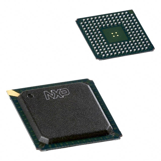
- Part No.:
- SAA7105E/V1/G,557
- Manufacturer:
- NXP Semiconductors
- Category:
- Encoders, Decoders, Converters
- Package:
- 156-LBGA
- Datasheet:
-
 SAA7105E/V1/G,557.pdf
- Description:
- IC DIGITAL VIDEO ENCODER 156LBGA
- Quantity:
- Payment:

- Shipping:

Inventory:4,227
Please send an inquiry. Send us your inquiry, and we will respond immediately.
Product details
Overview
SAA7105E/V1/G,557 from NXP Semiconductors (formerly Philips Semiconductors) is a monolithic 3.3 V CMOS digital video encoder IC that converts non-interlaced RGB or 4:2:2 Y-CB-CR graphics data up to 1280 × 1024 @ 60 Hz into analog PAL/NTSC CVBS, S-video, or RGB-SCART outputs. It integrates a 27 MHz crystal oscillator, triple 10-bit DACs, programmable horizontal/vertical scaler, 5-line anti-flicker filter, and I²C-bus interface - enabling direct connection to PC graphics controllers for legacy TV output in industrial display and embedded multimedia systems.
For engineers reviewing the SAA7105E/V1/G,557 datasheet, SAA7105E/V1/G,557 pinout, SAA7105E/V1/G,557 application, or SAA7105E/V1/G,557 equivalent, key selection criteria include its 85 MHz maximum pixel clock support, 10-bit DAC linearity (±3 LSB integral, ±1 LSB differential), 3.15–3.45 V analog/digital supply tolerance, JTAG boundary scan test capability, and hardware cursor overlay for UI overlays in kiosk and medical display systems.
Technical Context
The SAA7105E/V1/G,557 implements a full digital video encoding pipeline: input formatter accepts RGB or Y-CB-CR formats (including ITU-R BT.656), routes data through RGB LUT gamma correction and cursor insertion, then applies horizontal scaling (XINC/4096 resolution) and vertical scaling with re-interlacing. Its encoder block generates crystal-stable 13.5 MHz subcarrier signals independent of input pixel clock, with luminance interpolated to 27 MHz and chrominance processed at 6.75 MHz before quadrature modulation.
Timing generation is fully synchronized to an on-chip 27 MHz oscillator (fundamental or 3rd-harmonic crystal), supporting both master and slave I²C-bus operation at 400 kHz. The device features dedicated hot-plug detection (TVD pin), programmable sync phase alignment (HSVGC/VSVGC/FSVGC), and optional teletext/VPS/closed caption insertion on line 21/23/20 - all while maintaining 5 V-tolerant I/Os for compatibility with legacy 5 V graphics interfaces.
Key Specifications
| Parameter | Value and Actual Design Meaning |
|---|---|
| Supply Voltage | 3.15–3.45 V for both analog (VDDA) and digital (VDDD) domains - ensures stable operation across industrial temperature range without external regulation. |
| DAC Resolution | 10-bit per channel (BLUE/CB/CVBS, GREEN/VBS/CVBS, RED/CR/C/CVBS) - delivers 1024-level grayscale and color fidelity for broadcast-compliant analog outputs. |
| Max Input Pixel Clock | 85 MHz (double-edged) - supports VGA up to 1280×1024@60 Hz and HDTV up to 1920×1080i@60 Hz without external clock synthesis. |
| Scaler Range | 50–400% down/upscaling - enables precise underscan/overscan control and adaptive display sizing for CRT and composite monitors. |
| I²C Interface Speed | 400 kHz Fast-mode - allows real-time register programming of video parameters (sync phase, border color, cursor position) during active display. |
| Anti-Flicker Filter | Programmable 5-line vertical filter - suppresses interlace flicker in PAL/NTSC outputs while preserving sharpness via adjustable YSKIP and weighting coefficients. |
| Crystal Oscillator | On-chip 27 MHz oscillator (fundamental or 3rd-harmonic) - eliminates need for external PLL, reduces BOM count, and guarantees subcarrier frequency stability per ITU-R BT.470-3. |
Pinout & Package
Package: BGA156 (SOT472-1), 15 × 15 × 1.15 mm body, 156-ball array - designed for high-density PCB layouts with thermal pad grounding and low-inductance power delivery.
| Pin/Terminal | Circuit Role | Design Meaning |
|---|---|---|
| PD0–PD11 | Parallel digital video input bus | 12-bit multiplexed RGB/Y-CB-CR data path; supports double-edge sampling for 27 MB/s throughput in 4:2:2 mode. |
| PIXCLKI / PIXCLKO | Pixel clock loop-through interface | Enables VGC synchronization: input feeds internal synthesizer, output drives graphics controller - critical for jitter-free timing in dual-display configurations. |
| BLUE_CB_CVBS / GREEN_VBS_CVBS / RED_CR_C_CVBS | Analog video outputs | Three independent 10-bit DAC outputs; each configurable as CVBS, S-video component (Y/CB/CR), or RGB+sync for SCART - no external reconstruction filters required. |
| TVD | TV detection interrupt | Active-low open-drain signal asserts when DAC output load is detected - enables automatic display mode switching without polling. |
| SDA / SCL | I²C-bus control interface | Fast-mode (400 kHz) bidirectional control port for configuring registers, loading LUTs, and uploading cursor bitmaps in-system. |
| TRST / TDI / TDO / TMS / TCK | JTAG boundary scan pins | IEEE 1149.1-compliant test interface - supports production testing, board-level diagnostics, and firmware validation without physical probe access. |
Key Features
| Feature | Design Value |
|---|---|
| Integrated 27 MHz oscillator | Eliminates external crystal oscillator circuitry and reduces layout sensitivity to EMI - improves time-to-market for cost-sensitive consumer electronics designs. |
| Hardware cursor overlay | 32×32 pixel, 2-bit-per-pixel cursor with programmable hot spot and color registers - offloads GUI rendering from host CPU and enables responsive pointer interaction in embedded OS environments. |
| RGB Look-Up Table (LUT) | 3×256-byte RAM-based gamma correction table loaded via I²C or pixel data port - enables per-channel tone mapping without host processor intervention. |
| Programmable border generator | Fills underscan area with user-defined RGB color - prevents black borders on overscanning TVs and maintains visual continuity in kiosk and signage applications. |
| Teletext/VPS/Closed Caption insertion | Real-time insertion of WST/NABTS data on line 21/23/20 at 27 MHz clock rate - supports regulatory compliance and interactive broadcast features in set-top box reference designs. |
Applications
| Industrial Display Terminal | Medical Imaging Monitor |
|---|---|
Use Scenario: Embedded PC in diagnostic ultrasound or patient monitor displays legacy VGA graphics on analog CRT/LCD panels with PAL/NTSC compliance. IC Role / Device Role / Timing Role: Digital video encoder converting non-interlaced 1024×768 graphics to interlaced CVBS output with precise 50/60 Hz frame locking and subcarrier stability. Use Value: Enables FDA-cleared medical devices to reuse existing analog display infrastructure while meeting IEC 60601-1 EMC and timing accuracy requirements via on-chip 27 MHz oscillator. |
Use Scenario: PACS workstation outputs DICOM images to secondary analog review monitors via SCART or composite video. IC Role / Device Role / Timing Role: Triple DAC outputs RGB + TTL sync with <±3 LSB integral linearity - preserves grayscale fidelity critical for radiological interpretation. Use Value: Eliminates external DACs and reconstruction filters, reducing analog signal path noise and ensuring consistent 10-bit luminance reproduction across clinical imaging deployments. |
| Kiosk & Digital Signage | Legacy Graphics Adapter |
Use Scenario: Self-service retail kiosk uses embedded x86 platform to drive multiple analog displays (CVBS + RGB) simultaneously with branded UI overlays. IC Role / Device Role / Timing Role: Hardware cursor and border generator provide real-time UI elements without GPU resource consumption; supports 1280×1024@60 Hz native resolution scaling. Use Value: Reduces host CPU load by >15% in Linux framebuffer mode and enables seamless branding via programmable underscan fill color - critical for 24/7 unattended operation. |
Use Scenario: Industrial motherboard adds NTSC/PAL video output to legacy ISA/PCI graphics controllers lacking integrated encoders. IC Role / Device Role / Timing Role: Acts as drop-in video bridge: accepts DVO-level RGB inputs (1.1–3.6 V), performs format conversion, and outputs standard-compliant CVBS/S-video. Use Value: Extends lifecycle of mature graphics IP by adding broadcast video capability without redesigning core logic - validated for Intel DVO interface timing compliance. |
Equivalent & Alternatives
The following parts are listed as comparable options for similar digital video encoder applications.
| Alternative Part | Technical Difference | Application Difference | Selection Advice |
|---|---|---|---|
| ADV7170KSTZ | Single 10-bit DAC, no integrated scaler or LUT; requires external clock synthesis and separate sync generator. | Limited to fixed-resolution CVBS output; lacks hardware cursor, teletext, and anti-flicker filtering - suitable only for basic video passthrough. | Select ADV7170KSTZ only when system already provides pixel clock, scaling, and UI overlay functions externally - avoids redundancy but increases BOM and layout complexity. |
| THS8135IPFP | Triple 10-bit DAC with integrated sync generator but no on-chip oscillator or JTAG; supports only RGB→CVBS, no Y-CB-CR input path. | No native ITU-R BT.656 support or programmable anti-flicker filter - requires external deinterlacer for DVD source integration. | Choose THS8135IPFP for RGB-only systems needing higher analog output drive strength (40 mA vs. SAA7105E's 20 mA), but verify external crystal and timing control availability. |
Compared with ADV7170KSTZ and THS8135IPFP, the SAA7105E/V1/G,557 delivers full self-contained video encoding - including scaler, oscillator, LUT, cursor, and JTAG - making it optimal for space-constrained, single-chip embedded video solutions where design consolidation and long-term supply stability are critical.
Availability
SAA7105E/V1/G,557 is available at Aetrix Electronics and suitable for industrial display terminals, medical imaging monitors, kiosk systems, and legacy graphics adapter designs requiring stable component supply with guaranteed long-term availability and traceable sourcing.
Supply support for SAA7105E/V1/G,557 includes scheduled delivery planning, volume procurement assistance, BOM continuity management, traceable sourcing, and lifecycle availability coordination for OEM customers, industrial embedded developers, connected-device designers, and electronics production programs.
Manufacturer
NXP Semiconductors is a global semiconductor leader focused on secure connectivity solutions for automotive, industrial, and IoT applications - formed from the spin-off of Philips Semiconductors in 2006.
The SAA7105E/V1/G,557 belongs to NXP's legacy video processing portfolio, designed specifically for bridging high-resolution digital graphics to analog broadcast video standards in cost-sensitive, reliability-critical embedded systems.
FAQ
What video standards does the SAA7105E/V1/G,557 support?
The SAA7105E/V1/G,557 supports PAL B/G and NTSC M encoding with crystal-stable 13.5 MHz subcarrier generation, compliant with RS-170-A and ITU-R BT.470-3 standards. It outputs CVBS, S-video (Y/CB/CR), and RGB+composite sync for SCART connectors - all at native 50 Hz or 60 Hz frame rates without external timing components. The SAA7105E/V1/G,557 does not support SECAM or digital HDMI/DisplayPort standards.
Does the SAA7105E/V1/G,557 require an external crystal?
No, the SAA7105E/V1/G,557 integrates a 27 MHz crystal oscillator supporting both fundamental and 3rd-harmonic crystals - eliminating the need for external oscillator circuitry. The XTALI and XTALO pins connect directly to a 27 MHz crystal, and the internal oscillator provides clocking for the DACs, encoder, and I²C-bus interface. This reduces BOM count and improves timing stability versus discrete oscillator solutions.
Can the SAA7105E/V1/G,557 output RGB and CVBS simultaneously?
Yes, the SAA7105E/V1/G,557 supports simultaneous RGB and CVBS output via its three independent DAC channels: BLUE_CB_CVBS, GREEN_VBS_CVBS, and RED_CR_C_CVBS. Each output can be configured independently - for example, BLUE_CB_CVBS and GREEN_VBS_CVBS driven as CVBS composite, while RED_CR_C_CVBS outputs RGB red - enabling multi-format display support from a single IC without external muxing.
What is the function of the TVD pin on the SAA7105E/V1/G,557?
The TVD pin on the SAA7105E/V1/G,557 is an active-low open-drain interrupt output that asserts when a valid analog load (e.g., TV or monitor) is detected at the DAC outputs. It enables hot-plug detection without software polling, allowing the host system to automatically enable video output, configure timing, or switch display modes upon connection - a key feature for kiosk and embedded systems requiring zero-touch setup.
Is the SAA7105E/V1/G,557 pin-compatible with the SAA7104E?
Yes, the SAA7105E/V1/G,557 is pin-compatible with the SAA7104E in the BGA156 package (SOT472-1) and shares identical pinout, electrical characteristics, and functional blocks. The primary difference is Macrovision™ copy protection support - present only in the SAA7104E - making the SAA7105E/V1/G,557 suitable for applications where content protection is not required, with identical PCB layout and firmware compatibility.
SAA7105E/V1/G,557 Specifications
- Product attributes
- Attribute value
- Manufacturer:
- NXP Semiconductors
- Series:
- -
- Package/Case:
- 156-LBGA
- Packaging:
- Tray
- Product Status:
- Obsolete
- Type:
- Video Encoder
- Applications:
- TV
- Voltage - Supply, Analog:
- 3.15V ~ 3.45V
- Voltage - Supply, Digital:
- 3.15V ~ 3.45V
- Grade:
- -
- Qualification:
- -
- Mounting Type:
- Surface Mount
- Supplier Device Package:
- 156-LBGA (15x15)
SAA7105E/V1/G,557 FAQ
1.How can I place an order for SAA7105E/V1/G,557 through Aetrix?
Please submit a Request for Quotation (RFQ) for SAA7105E/V1/G,557 on Aetrix. Our sales agent will provide a competitive quotation and guide you through the order confirmation once you accept the terms.
2.Are the price and stock information for SAA7105E/V1/G,557 reliable?
The price and inventory of SAA7105E/V1/G,557 are updated periodically and may fluctuate due to market conditions. Stock and pricing data are typically refreshed every 24 hours. Quotation validity for SAA7105E/V1/G,557 is usually 5 days.
3.What payment methods are accepted for SAA7105E/V1/G,557?
We accept Wire Transfer, PayPal, Credit Card, Western Union, MoneyGram, and Escrow for SAA7105E/V1/G,557 transactions.
Note: Certain payment methods may incur a processing fee.
4.How is shipping managed for SAA7105E/V1/G,557?
SAA7105E/V1/G,557 orders can be shipped via leading logistics carriers, including DHL, UPS, FedEx, TNT, or Registered Mail.
Once your SAA7105E/V1/G,557 order is processed, you will receive an email with the shipment details and tracking number.
Note: Tracking information may take up to 24 hours to appear. Express delivery typically takes 3–5 business days.
5.How can I obtain technical support or documentation for SAA7105E/V1/G,557?
For technical support, including SAA7105E/V1/G,557 datasheets, pinout diagrams, or application guidance, please contact our engineering support team. They can provide detailed documentation and assistance for your SAA7105E/V1/G,557 requirements.
6.How does Aetrix verify that SAA7105E/V1/G,557 is sourced from the original manufacturer or authorized distributors?
All SAA7105E/V1/G,557 products on Aetrix are procured from qualified distributors and authorized channels. Our dedicated quality assurance team conducts strict verification, including traceability checks and, if necessary, third-party testing. This ensures that SAA7105E/V1/G,557 meets industry standards.
7.What is the process for return or replacement of SAA7105E/V1/G,557?
All SAA7105E/V1/G,557 units undergo pre-shipment inspection (PSI). If there is an issue with SAA7105E/V1/G,557, returns or replacements are accepted under the following conditions:
1.Quantity discrepancies, incorrect items, or visible external defects (such as breakage or corrosion), acknowledged by Aetrix.
2.The issue is reported within 90 days of delivery.
3.The SAA7105E/V1/G,557 part is unused and in its original packaging.
Return procedure for SAA7105E/V1/G,557:
1.Submit a request within 90 days.
2.Obtain a Return Material Authorization (RMA) from Aetrix.
SAA7105E/V1/G,557 Tags

-
MCP2120T-I/SL
Microchip Technology

-
LICAL-ENC-MS001
TE Connectivity Linx
-
TW9990AT-NA1-GR
Renesas
-
TVP5151IPBSR
Texas Instruments
-
TVP5150AM1IPBSR
Texas Instruments
-
LICAL-DEC-MS001-T
TE Connectivity Linx
-
ADV7391BCPZ
Analog Devices Inc.
-
ADV7393BCPZ-REEL
Analog Devices Inc.
-
ADV7393BCPZ
Analog Devices Inc.
-
ADV7391WBCPZ
Analog Devices Inc.
-
ADV7181DBCPZ
Analog Devices Inc.

-
ADV7181CBSTZ-REEL
Analog Devices Inc.
Tech Hub

A practical engineering guide to 3.3V and 5V logic compatibility, input thresholds, resistor dividers, translator ICs, MOSFET level shifting, I2C pull-ups, timing limits and power-sequencing risks.

The 74HC595 uses push-pull logic outputs, while the TPIC6B595 uses 50 V open-drain DMOS sinks for higher-power loads. This guide compares timing, current limits, 3.3 V interfacing, load wiring, thermal…

The 74HC595 converts serial data into eight stable parallel outputs. This guide covers pin functions, shift and storage timing, OE and MR behavior, drive-current limits, cascading, voltage compatibilit…

A technical comparison of level-sensitive latches and edge-triggered flip-flops, covering timing windows, setup and hold limits, master–slave operation, time borrowing, race-through, HDL inference and…

A D latch stores one bit while Enable controls when data can pass. This reference covers gate-level operation, truth tables, transparency, setup and hold timing, LE versus OE, common ICs and practical …

An SR latch stores one bit through cross-coupled feedback. This engineering reference covers NOR and NAND implementations, truth tables, forbidden-state recovery, gated operation, switch debouncing, fa…

Latch circuits retain one bit through feedback. This technical reference covers SR and D latches, truth tables, transparency, timing limits, latch-versus-flip-flop behavior, applications and common log…

An engineering guide to LED driver operation, constant-current and constant-voltage outputs, linear and switching topologies, dimming, IC selection, calculations, replacement compatibility, and fault c…

Operational amplifier guide covering op amp basics, feedback, ideal vs real op amps, common configurations, buffer circuits, offset, bias current, gain-bandwidth, slew rate, rail-to-rail limits and sel…

Jumper cables guide covering safe connection order, red and black clamp placement, final ground connection, cable gauge, length, clamp quality, copper vs CCA cables, jump starter comparison and battery…


