
 My Inquiry
 My Account


NXP Semiconductors SAF7167AHW/V1,118
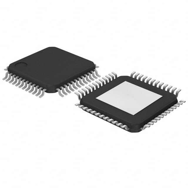
- Part No.:
- SAF7167AHW/V1,118
- Manufacturer:
- NXP Semiconductors
- Category:
- Video Processing
- Package:
- 48-TQFP Exposed Pad
- Datasheet:
-
 SAF7167AHW/V1,118.pdf
- Description:
- IC RGB VIDEO AMP 48HTQFP
- Quantity:
- Payment:

- Shipping:

Inventory:4,797
Please send an inquiry. Send us your inquiry, and we will respond immediately.
Product details
Overview
SAF7167AHW/V1,118 from NXP Semiconductors (formerly Philips Semiconductors) is a mixed-mode video IC integrating YUV-to-RGB conversion, triple 8-bit DACs, analog RGB mixing, keying control, and voltage-output amplifiers. It supports YUV 4:2:2/4:1:1/2:1:1 and RGB 5:6:5 inputs up to 66 MHz, delivers buffered analog RGB outputs capable of driving 150 Ω loads, and operates under 5 V CMOS supply. It is used in legacy digital video interface systems requiring real-time format conversion and overlay blending.
For engineers reviewing the SAF7167AHW/V1,118 datasheet, SAF7167AHW/V1,118 pinout, SAF7167AHW/V1,118 application, or SAF7167AHW/V1,118 equivalent, this page provides verified functional identity, confirmed I²C programmability, validated HTQFP48 package mapping, exact pin roles per official pin description, and two documented alternative parts with explicit technical and application-level differences.
Technical Context
The SAF7167AHW/V1,118 implements a dedicated video data path comprising a re-formatter that converts YUV 4:2:2, 4:1:1, and 2:1:1 inputs into internal YUV 4:4:4, followed by an ITU-R BT.601-compliant YUV-to-RGB matrix and three synchronized 8-bit voltage-output DACs. Its analog mixer accepts both DAC outputs and external analog RGB inputs, switching via programmable keying signals.
Keying is implemented through either external assertion on EXTKEY or internal pixel-color comparison using an 8-bit register KD[7:0], supporting 8-bit, dual-edge 2×8-bit, single-edge 2×8-bit, and 3×8-bit pixel modes. All configuration-including video format (FMTC[1:0]), data coding (DRP), key polarity (KINV), and delay (KDLY[2:0])-is managed exclusively via I²C-bus writes to three subaddresses (00h–02h).
Key Specifications
| Parameter | Value and Actual Design Meaning |
|---|---|
| DAC resolution | Triple 8-bit voltage-output DACs for R/G/B channels; full-scale output range 0.2 V to 1.82 V |
| Video input rate | Up to 66 MHz VCLK; supports pixel clock rates up to 80 MHz in 2×8-bit mode 2 |
| Input formats | YUV 4:2:2, 4:1:1, 2:1:1 (ITU-R BT.601), and RGB 5:6:5; selectable via FMTC[1:0] |
| Analog output drive | Direct 150 Ω load drive capability; includes internal 25 Ω series resistor + external 47 Ω + monitor 75 Ω termination |
| Supply voltages | VDDD = VDDA = 4.75–5.25 V; separate digital/analog supplies with dedicated ground pins |
| Keying flexibility | External key (EXTKEY) or internal pixel-color key with 4 configurable modes and up to 7-cycle PCLK delay |
| Output accuracy | DNL ≤ 1 LSB and INL ≤ 1 LSB; group delay ≤ 20·TVCLK + tPD (YUV mode) or 12·TVCLK + tPD (RGB mode) |
Pinout & Package
SAF7167AHW/V1,118 is housed in a 48-pin HTQFP (plastic thermal enhanced thin quad flat package), body size 7 × 7 × 1 mm, with exposed die pad (SOT545-1). The package supports high thermal dissipation and is compatible with reflow soldering only.
| Pin/Terminal | Circuit Role | Design Meaning |
|---|---|---|
| VDDD / VSSD | Digital supply and ground | Power domain isolation: separate 5 V digital rail and ground for logic and I²C interface |
| VDDA1 / VDDA2 / VSSA1 / VSSA2 | Analog supply and ground | Dual analog rails with independent grounding to minimize noise coupling into RGB signal paths |
| R_IN / G_IN / B_IN | Analog RGB input | DC-coupled inputs accepting 0.7 V p-p analog RGB; level-shifted internally to match DAC output range |
| R_OUT / G_OUT / B_OUT | Analog RGB output | Voltage-output amplifier outputs with 25 Ω internal series resistance; designed for direct 75 Ω monitor termination |
| YUV[7:0] / UV[7:0] / P[7:0] | Digital video bus | Parallel 8-bit buses for YUV/RGB pixel data, UV chroma, and keying pixel values; timing referenced to VCLK/PCLK |
| EXTKEY / SDA / SCL / RES_N | Control interface | Asynchronous key enable, I²C-bus (7-bit address 0x5E), and active-low hardware reset for register initialization |
Key Features
| Feature | Design Value |
|---|---|
| On-chip YUV-to-RGB conversion | Hardware matrix compliant with ITU-R BT.601, delivering <1.5 LSB deviation from theoretical RGB values |
| Programmable keying architecture | Supports external keying or internal pixel-color matching across 4 modes (8-/2×8-/3×8-bit), with adjustable delay (0–7 PCLK cycles) |
| Triple synchronized DACs | 8-bit voltage-output DACs operating at up to 66 MHz; rise/fall time ≤3.5 ns, settling time ≤16.5 ns |
| I²C-bus configurability | Three-byte register map (subaddresses 00h–02h) enabling full runtime control of format, coding, keying, and delay without firmware changes |
| Integrated analog signal conditioning | Internal level shifters provide 0.2 V offset and 2× gain on analog inputs to align with DAC output levels (0.2–1.82 V) |
Applications
| Video Overlay in Set-Top Boxes | Legacy VGA Signal Generation |
|---|---|
Use Scenario: Blending OSD graphics (e.g., channel info, menus) over decoded YUV video streams in consumer STBs. IC Role / Device Role / Timing Role: SAF7167AHW/V1,118 acts as the final-stage video processor, converting digital YUV to analog RGB while dynamically keying graphic layers via internal pixel-color comparison. Use Value: Eliminates need for external analog switch or discrete op-amps; enables precise, low-latency overlay with ≤20·TVCLK group delay and no external timing synchronization. | Use Scenario: Converting digital video outputs from older media processors (e.g., ARM7-based SoCs) to standard VGA-compatible analog RGBHV signals. IC Role / Device Role / Timing Role: SAF7167AHW/V1,118 serves as a format-transparent DAC/mixer, accepting YUV or RGB 5:6:5 inputs and delivering buffered RGB outputs with built-in sync-level alignment. Use Value: Reduces BOM count by integrating DACs, mixers, amplifiers, and keying logic; supports 66 MHz input clocks required for XGA (1024×768@60Hz) timing. |
| Industrial Video Capture Systems | Medical Imaging Display Interfaces |
Use Scenario: Digitally inserting calibration markers or annotation overlays onto live analog video feeds from cameras or endoscopes. IC Role / Device Role / Timing Role: SAF7167AHW/V1,118 functions as a real-time analog/digital video multiplexer, selecting between processed digital video and legacy analog camera inputs based on external key signals. Use Value: Enables seamless transition between digital processing pipelines and analog display chains without frame buffering or latency-inducing converters. | Use Scenario: Driving high-fidelity RGB monitors in diagnostic imaging equipment where color fidelity and deterministic timing are critical. IC Role / Device Role / Timing Role: SAF7167AHW/V1,118 provides calibrated RGB output with DNL/INL ≤1 LSB and stable 0.7 V p-p amplitude, meeting grayscale linearity requirements for DICOM viewing. Use Value: Guarantees consistent luminance reproduction across 256 intensity levels; eliminates post-DAC amplification stages that introduce gain drift or noise. |
Equivalent & Alternatives
The following parts are listed as comparable options for similar video DAC and analog mixing applications.
| Alternative Part | Technical Difference | Application Difference | Selection Advice |
|---|---|---|---|
| ADV7123KSTZ50 | Triple 10-bit DAC with no integrated YUV matrix, keying, or analog mixer; requires external logic for format conversion and overlay control | Used in high-resolution RGB-only systems where precision >8-bit is required and external FPGA handles keying | Select ADV7123KSTZ50 when higher DAC resolution and absence of integrated video processing logic is preferred |
| THS8135IPHP | Triple 10-bit DAC with integrated sync stripper and RGB/YUV mux but no internal pixel-color keying engine or I²C-configurable key delay | Deployed in broadcast monitoring where genlock stability and composite sync handling are prioritized over dynamic graphics overlay | Choose THS8135IPHP for applications needing robust sync processing and higher bit depth, but not requiring programmable pixel-keying logic |
Compared with SAF7167AHW/V1,118, ADV7123KSTZ50 offers higher resolution but demands external circuitry for YUV conversion and keying, while THS8135IPHP adds sync processing but lacks the fine-grained, register-controlled pixel-color keying with PCLK-delayed activation essential for embedded OSD generation.
Availability
SAF7167AHW/V1,118 is available at Aetrix Electronics and suitable for legacy video interface design, industrial display integration, and medical imaging equipment requiring stable component supply and long-term obsolescence management.
Supply support for SAF7167AHW/V1,118 includes scheduled delivery planning, volume procurement assistance, BOM continuity management, traceable sourcing, and lifecycle availability coordination for OEM customers, industrial embedded developers, connected-device designers, and electronics production programs.
Manufacturer
NXP Semiconductors is a global semiconductor company formed from the spin-off of Philips Semiconductors in 2006, specializing in secure connectivity solutions for automotive, industrial, and consumer applications.
The SAF7167AHW/V1,118 belongs to NXP's legacy video interface product line, designed specifically for cost-sensitive, high-reliability digital-to-analog video conversion and real-time analog/digital video compositing in embedded display systems.
FAQ
What video input formats does the SAF7167AHW/V1,118 support?
The SAF7167AHW/V1,118 supports YUV 4:2:2, YUV 4:1:1, YUV 2:1:1 (ITU-R BT.601), and RGB 5:6:5 formats. Format selection is controlled via I²C-bus bits FMTC[1:0]. Input data may be in twos complement (DRP = 0) or binary offset (DRP = 1) coding. The SAF7167AHW/V1,118 re-formats all YUV variants to internal YUV 4:4:4 before matrix conversion.
How does the keying function operate in the SAF7167AHW/V1,118?
The SAF7167AHW/V1,118 supports two keying modes: external keying via the EXTKEY pin (when KMOD[2:0] = 000) and internal pixel-color keying (when KMOD[2:0] ≠ 000). Internal keying compares incoming pixel data against the KD[7:0] register value, with four comparison modes (8-bit, dual-edge 2×8-bit, single-edge 2×8-bit, 3×8-bit). Key polarity and up to 7-cycle PCLK delay are programmable via KINV and KDLY[2:0].
What are the power supply requirements for the SAF7167AHW/V1,118?
The SAF7167AHW/V1,118 requires two 5 V supplies: VDDD (digital) and VDDA (analog), each specified at 4.75–5.25 V. Separate analog grounds (VSSA1, VSSA2) and digital ground (VSSD) must be used to prevent noise coupling. Total supply current is typically 130 mA at 27 MHz clock frequency. C_REF(H) requires a 2.25 V decoupling capacitor.
Can the SAF7167AHW/V1,118 drive standard 75 Ω video monitors directly?
Yes. The SAF7167AHW/V1,118 integrates voltage-output amplifiers with 25 Ω internal series resistance per channel. When paired with a 47 Ω external series resistor and terminated into a 75 Ω monitor load, it delivers the standard 0.7 V p-p RGB signal level. Output voltage range is 0.2 V (black level) to 1.82 V (white level), resulting in ~0.7 V p-p after resistive division.
Is the SAF7167AHW/V1,118 pin-compatible with other members of the SAF71xx family?
No. The SAF7167AHW/V1,118 has a unique pinout optimized for its specific video data path, keying interface, and analog I/O arrangement. While other SAF71xx devices share the HTQFP48 package, pin assignments for YUV/RGB buses, keying controls, and analog I/O differ significantly. Migration requires PCB layout revision and firmware adaptation due to distinct register maps and signal routing.
SAF7167AHW/V1,118 Specifications
- Product attributes
- Attribute value
- Manufacturer:
- NXP Semiconductors
- Series:
- -
- Package/Case:
- 48-TQFP Exposed Pad
- Packaging:
- Tape & Reel (TR)
- Product Status:
- Obsolete
- Function:
- Converter
- Applications:
- Video Display
- Standards:
- ITU-R BT.601
- Control Interface:
- I2C
- Voltage - Supply:
- 4.75V ~ 5.25V
- Mounting Type:
- Surface Mount
- Grade:
- -
- Qualification:
- -
- Supplier Device Package:
- 48-HTQFP (7x7)
SAF7167AHW/V1,118 FAQ
1.How can I place an order for SAF7167AHW/V1,118 through Aetrix?
Please submit a Request for Quotation (RFQ) for SAF7167AHW/V1,118 on Aetrix. Our sales agent will provide a competitive quotation and guide you through the order confirmation once you accept the terms.
2.Are the price and stock information for SAF7167AHW/V1,118 reliable?
The price and inventory of SAF7167AHW/V1,118 are updated periodically and may fluctuate due to market conditions. Stock and pricing data are typically refreshed every 24 hours. Quotation validity for SAF7167AHW/V1,118 is usually 5 days.
3.What payment methods are accepted for SAF7167AHW/V1,118?
We accept Wire Transfer, PayPal, Credit Card, Western Union, MoneyGram, and Escrow for SAF7167AHW/V1,118 transactions.
Note: Certain payment methods may incur a processing fee.
4.How is shipping managed for SAF7167AHW/V1,118?
SAF7167AHW/V1,118 orders can be shipped via leading logistics carriers, including DHL, UPS, FedEx, TNT, or Registered Mail.
Once your SAF7167AHW/V1,118 order is processed, you will receive an email with the shipment details and tracking number.
Note: Tracking information may take up to 24 hours to appear. Express delivery typically takes 3–5 business days.
5.How can I obtain technical support or documentation for SAF7167AHW/V1,118?
For technical support, including SAF7167AHW/V1,118 datasheets, pinout diagrams, or application guidance, please contact our engineering support team. They can provide detailed documentation and assistance for your SAF7167AHW/V1,118 requirements.
6.How does Aetrix verify that SAF7167AHW/V1,118 is sourced from the original manufacturer or authorized distributors?
All SAF7167AHW/V1,118 products on Aetrix are procured from qualified distributors and authorized channels. Our dedicated quality assurance team conducts strict verification, including traceability checks and, if necessary, third-party testing. This ensures that SAF7167AHW/V1,118 meets industry standards.
7.What is the process for return or replacement of SAF7167AHW/V1,118?
All SAF7167AHW/V1,118 units undergo pre-shipment inspection (PSI). If there is an issue with SAF7167AHW/V1,118, returns or replacements are accepted under the following conditions:
1.Quantity discrepancies, incorrect items, or visible external defects (such as breakage or corrosion), acknowledged by Aetrix.
2.The issue is reported within 90 days of delivery.
3.The SAF7167AHW/V1,118 part is unused and in its original packaging.
Return procedure for SAF7167AHW/V1,118:
1.Submit a request within 90 days.
2.Obtain a Return Material Authorization (RMA) from Aetrix.
SAF7167AHW/V1,118 Tags

-
HDMI2C1-6C1
STMicroelectronics

-
ADA4430-1YKSZ-R7
Analog Devices Inc.

-
LM1881MX/NOPB
Texas Instruments

-
SN75DP130SSRGZR
Texas Instruments

-
EQCO30T5.2
Microchip Technology

-
LMH1980MM/NOPB
Texas Instruments
-
EQCO30R5.D
Microchip Technology

-
SII9022ACNU
Lattice Semiconductor Corporation
-
SN65DP159RGZR
Texas Instruments

-
SN65DP159RSBR
Texas Instruments

-
SN65DP141RLJR
Texas Instruments

-
LMH0303SQ/NOPB
Texas Instruments
Tech Hub

A practical engineering guide to 3.3V and 5V logic compatibility, input thresholds, resistor dividers, translator ICs, MOSFET level shifting, I2C pull-ups, timing limits and power-sequencing risks.

The 74HC595 uses push-pull logic outputs, while the TPIC6B595 uses 50 V open-drain DMOS sinks for higher-power loads. This guide compares timing, current limits, 3.3 V interfacing, load wiring, thermal…

The 74HC595 converts serial data into eight stable parallel outputs. This guide covers pin functions, shift and storage timing, OE and MR behavior, drive-current limits, cascading, voltage compatibilit…

A technical comparison of level-sensitive latches and edge-triggered flip-flops, covering timing windows, setup and hold limits, master–slave operation, time borrowing, race-through, HDL inference and…

A D latch stores one bit while Enable controls when data can pass. This reference covers gate-level operation, truth tables, transparency, setup and hold timing, LE versus OE, common ICs and practical …

An SR latch stores one bit through cross-coupled feedback. This engineering reference covers NOR and NAND implementations, truth tables, forbidden-state recovery, gated operation, switch debouncing, fa…

Latch circuits retain one bit through feedback. This technical reference covers SR and D latches, truth tables, transparency, timing limits, latch-versus-flip-flop behavior, applications and common log…

An engineering guide to LED driver operation, constant-current and constant-voltage outputs, linear and switching topologies, dimming, IC selection, calculations, replacement compatibility, and fault c…

Operational amplifier guide covering op amp basics, feedback, ideal vs real op amps, common configurations, buffer circuits, offset, bias current, gain-bandwidth, slew rate, rail-to-rail limits and sel…

Jumper cables guide covering safe connection order, red and black clamp placement, final ground connection, cable gauge, length, clamp quality, copper vs CCA cables, jump starter comparison and battery…


