
 My Inquiry
 My Account


NXP Semiconductors SC16C550BIBS128
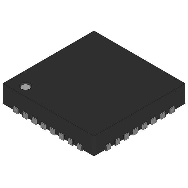
- Part No.:
- SC16C550BIBS128
- Manufacturer:
- NXP Semiconductors
- Package:
- 32-VFQFN Exposed Pad
- Datasheet:
-
 SC16C550BIBS128.pdf
- Description:
- SERIAL I/O CONTROLLER 1 CHANNEL
- Quantity:
- Payment:

- Shipping:

Inventory:4,370
Please send an inquiry. Send us your inquiry, and we will respond immediately.
Product details
Overview
SC16C550BIBS128 from NXP Semiconductors is a 32-pin HVQFN-packaged Universal Asynchronous Receiver and Transmitter (UART) IC that converts parallel CPU data to serial streams and vice versa, supporting up to 3 Mbit/s at 5 V, 2 Mbit/s at 3.3 V, and 1 Mbit/s at 2.5 V. It integrates 16-byte transmit and receive FIFOs, programmable auto-RTS/CTS hardware flow control, and full modem interface signals (CTS, RTS, DTR, DSR, DCD, RI), enabling robust serial communication in industrial embedded systems.
For engineers reviewing the SC16C550BIBS128 datasheet, SC16C550BIBS128 pinout, SC16C550BIBS128 application, or SC16C550BIBS128 equivalent, key selection considerations include its HVQFN32 package footprint, absence of TXRDY/RXRDY signals (not supported in this variant), 5/3.3/2.5 V dual-supply operation, FIFO trigger level configurability, and compatibility with legacy 16C450 software stacks.
Technical Context
The SC16C550BIBS128 implements a register-compatible extension of the industry-standard 16C450 UART architecture, with enhanced FIFO buffering and hardware flow control logic. Its internal baud rate generator accepts up to 48 MHz clock input and divides by programmable 16-bit divisors to achieve precise serial rates-including 921.6 kbit/s standard and custom values-while BAUDOUT and RCLK are internally bonded in the HVQFN32 package.
It supports four receiver FIFO interrupt trigger levels (1/4/8/14 bytes), prioritized interrupt handling (transmit empty, receive ready, line status, modem status), and loopback diagnostics. The device operates across −40 °C to +85 °C and features 3-state TTL-compatible bus drivers for D0–D7, A0–A2, and control lines, with AS-address strobe enabling flexible memory-mapped or I/O-mapped CPU interfacing.
Key Specifications
| Parameter | Value and Actual Design Meaning |
|---|---|
| Supply Voltage | 2.5 V, 3.3 V, or 5 V ±10 % - enables direct integration into mixed-voltage industrial control boards without level-shifting. |
| Max Data Rate | 3 Mbit/s at 5 V - supports high-speed modem and networking interfaces requiring >1 Mbit/s throughput. |
| FIFO Depth | 16-byte TX and RX FIFOs - reduces CPU interrupt load by ~8× versus 1-byte 16C450, improving real-time response in multi-channel systems. |
| Operating Temp | −40 °C to +85 °C - qualified for industrial automation, motor drives, and outdoor communications equipment. |
| Package | HVQFN32 (5 × 5 × 0.85 mm) - compact thermal-enhanced footprint with exposed pad for PCB heat dissipation. |
| Interface Mode | Parallel CPU bus (8-bit D0–D7, A0–A2, CS/AS/IOR/IOW) - compatible with 8051, ARM, and FPGA host controllers via memory-mapped or I/O-mapped access. |
| Modem Signals | Full set: CTS, RTS, DTR, DSR, DCD, RI - enables direct connection to RS-232 transceivers and legacy telecom peripherals. |
Pinout & Package
HVQFN32 package (SOT617-1), 5 mm × 5 mm body, 0.5 mm pitch, 32 terminals, thermally enhanced with exposed center pad requiring soldering to PCB ground plane per NXP SOT617-1 mechanical spec.
| Pin/Terminal | Circuit Role | Design Meaning |
|---|---|---|
| D0–D7 | Data bus I/O | Bidirectional 8-bit parallel interface to CPU; 3-state outputs allow shared bus operation. |
| A0–A2 | Register address select | Selects among 8 internal registers (THR/RHR, IER/ISR, LCR/LSR, MCR/MSR, FCR, SPR, DLL/DLM) during read/write cycles. |
| CS | Chip select | Active-low enable for UART register access; replaces CS0/CS1/CS2 used in larger packages. |
| IOR / IOW | Read/write strobes | Separate active-low control for reading status/data or writing control words; supports standard 8080-style bus timing. |
| INT | Interrupt output | Open-drain or push-pull (configurable) signal indicating pending UART event: TX empty, RX ready, line error, or modem change. |
| TX / RX | Serial I/O | Asynchronous TTL-level transmit and receive data lines; require external RS-232/RS-485 transceiver for physical layer compliance. |
| RTS / CTS | Hardware flow control | Auto-RTS deactivates when RX FIFO reaches programmed trigger level; auto-CTS halts TX when CTS goes inactive mid-frame. |
| RESET | Master reset | Active-high asynchronous reset clearing all registers and initializing outputs to default states (e.g., TX HIGH, RTS/CTS HIGH). |
| XTAL1 / XTAL2 | Crystal oscillator interface | Supports 1.8432 MHz to 48 MHz crystal or external clock; BAUDOUT and RCLK internally bonded in HVQFN32. |
| VDD / VSS | Power supply | Single 2.5/3.3/5 V supply; VSS connected to both pin 9 and pin 13 plus exposed thermal pad - all must be grounded. |
Key Features
| Feature | Design Value |
|---|---|
| 16-byte TX/RX FIFOs | Reduces CPU interrupt frequency by up to 16× versus 16C450, lowering host processing overhead in real-time embedded applications. |
| Programmable auto-RTS/CTS | Eliminates RX FIFO overrun errors without software intervention; RTS deassertion triggered at 1/4/8/14-byte RX thresholds. |
| Four FIFO interrupt levels | Enables fine-grained latency vs. throughput trade-offs: low trigger (1 byte) for minimal delay; high trigger (14 bytes) for burst efficiency. |
| 16C450 software compatibility | Power-on reset configures registers identically to 16C450, allowing drop-in replacement in existing BIOS, OS drivers, and firmware stacks. |
| Independent TX/RX clocking | RCLK input allows separate receiver clock source (e.g., recovered clock from modem), decoupling RX timing from transmitter baud rate. |
Applications
| Industrial PLC Serial Port | Medical Device Data Logger |
|---|---|
Use Scenario: Serial interface between PLC main controller and field I/O modules using RS-485 physical layer. IC Role / Device Role / Timing Role: UART bridge converting parallel bus transactions to framed asynchronous serial packets with hardware flow control. Use Value: 16-byte FIFOs absorb bursty sensor data bursts; auto-RTS prevents buffer overflow during transient network congestion. | Use Scenario: ECG monitor transmitting patient waveform data to central nursing station over isolated RS-232 link. IC Role / Device Role / Timing Role: Asynchronous data converter with precise baud rate generation (e.g., 115.2 kbit/s) and line break detection for frame synchronization. Use Value: Programmable 5–8 bit character length and parity support ensures compatibility with legacy hospital IT protocols. |
| Point-of-Sale Terminal | Smart Energy Meter |
Use Scenario: Credit card reader interface in retail terminal communicating with payment gateway via RS-232. IC Role / Device Role / Timing Role: Secure serial data conduit with false start-bit rejection and framing error detection to prevent corrupted transaction data. Use Value: Full modem control (DTR/DSR/DCD/RI) enables handshake-based power management and peripheral presence detection. | Use Scenario: AMI (Advanced Metering Infrastructure) meter reporting consumption data to concentrator via GPRS modem. IC Role / Device Role / Timing Role: High-reliability UART with loopback diagnostics and temperature-hardened operation for outdoor deployment. Use Value: −40 °C to +85 °C rating and 2.5 V/3.3 V support match battery-backed meter power architecture and wide ambient ranges. |
Equivalent & Alternatives
The following parts are listed as comparable options for similar UART applications.
| Alternative Part | Technical Difference | Application Difference | Selection Advice |
|---|---|---|---|
| TL16C550CPM | 44-pin PLCC package; includes TXRDY/RXRDY DMA signals; no internal BAUDOUT–RCLK bond. | Requires larger PCB footprint; supports DMA-driven transfers not available in SC16C550BIBS128. | Select when DMA signaling and legacy PLCC socket compatibility are required over space-constrained HVQFN layout. |
| ST16C550CJ | 48-pin LQFP package; supports same 3 V/5 V operation and 16-byte FIFOs; pinout differs for CS/AS signals. | Needs board redesign for LQFP48; offers identical functional feature set but different package thermal profile. | Choose for higher thermal mass in high-ambient environments where HVQFN32 thermal pad implementation is impractical. |
Compared with TL16C550CPM and ST16C550CJ, the SC16C550BIBS128 trades DMA signaling and larger package options for ultra-compact HVQFN32 integration and simplified clock routing (bonded BAUDOUT/RCLK), making it optimal for space- and thermal-constrained industrial edge nodes.
Availability
SC16C550BIBS128 is available at Aetrix Electronics and suitable for industrial PLC serial ports, medical data loggers, point-of-sale terminals, and smart energy meters requiring stable component supply across extended temperature ranges and long production lifecycles.
Supply support for SC16C550BIBS128 includes scheduled delivery planning, volume procurement assistance, BOM continuity management, traceable sourcing, and lifecycle availability coordination for OEM customers, industrial embedded developers, connected-device designers, and electronics production programs.
Manufacturer
NXP Semiconductors is a global semiconductor leader focused on secure connectivity solutions for automotive, industrial, and IoT applications, with deep expertise in interface, power, and security ICs.
The SC16C550BIBS128 belongs to NXP's legacy industrial UART product line, designed specifically for reliable, software-compatible serial communication in harsh-environment embedded systems requiring long-term supply stability and broad voltage/temperature support.
FAQ
What is the maximum serial data rate supported by the SC16C550BIBS128?
The SC16C550BIBS128 supports up to 3 Mbit/s at 5 V, 2 Mbit/s at 3.3 V, and 1 Mbit/s at 2.5 V. This performance requires a 48 MHz input clock to the BAUDOUT/RCLK circuit. The actual achievable rate depends on the selected divisor value and crystal accuracy; for example, with a 1.8432 MHz crystal, standard rates like 115.2 kbit/s are achieved with zero error using divisor 12.
Does the SC16C550BIBS128 support hardware flow control, and how is it implemented?
Yes, the SC16C550BIBS128 supports programmable auto-RTS and auto-CTS hardware flow control. Auto-RTS asserts RTS when the RX FIFO falls below a user-configured trigger level (1/4/8/14 bytes); auto-CTS pauses transmission when CTS goes inactive mid-frame. Both functions are enabled via MCR[5] and MCR[1], eliminating software polling and preventing RX FIFO overrun in SC16C550BIBS128-based designs.
Why are TXRDY and RXRDY signals not available on the SC16C550BIBS128?
TXRDY and RXRDY signals are explicitly omitted in the HVQFN32 package variant of the SC16C550B, as confirmed in the NXP datasheet Section 5.2 Pin Description. These DMA-ready signals are present only in PLCC44, LQFP48, and DIP40 packages. The SC16C550BIBS128 relies on interrupt-driven or polling-based data transfer instead, consistent with its compact footprint optimization.
Is the SC16C550BIBS128 pin-compatible with older 16C450-based designs?
Yes, the SC16C550BIBS128 is functionally and register-compatible with the 16C450 after reset, and its HVQFN32 pinout maps core signals (D0–D7, A0–A2, IOR/IOW, INT, TX/RX, RTS/CTS, RESET, XTAL1/XTAL2, VDD/VSS) to dedicated pins. However, CS is consolidated to a single pin (replacing CS0/CS1/CS2), and AS is omitted - requiring minor PCB layout adaptation but preserving full software compatibility for SC16C550BIBS128 integration.
How does the SC16C550BIBS128 handle clocking, and what is the role of BAUDOUT and RCLK?
The SC16C550BIBS128 uses a single programmable baud rate generator fed by XTAL1 (crystal or external clock). BAUDOUT provides a 16× baud-rate output; in the HVQFN32 package, BAUDOUT and RCLK are internally bonded, meaning RCLK is driven by BAUDOUT - eliminating need for external connection. This simplifies clock routing and ensures synchronous TX/RX timing in SC16C550BIBS128 implementations.
SC16C550BIBS128 Specifications
- Product attributes
- Attribute value
- Manufacturer:
- NXP Semiconductors
- Package/Case:
- 32-VFQFN Exposed Pad
- Series:
- *
- Packaging:
- Bulk
- Product Status:
- Active
- Features:
- -
- Number of Channels:
- 1, UART
- FIFO's:
- 16 Byte
- Protocol:
- -
- Data Rate (Max):
- 3Mbps
- Voltage - Supply:
- 2.5V, 3.3V, 5V
- With Auto Flow Control:
- Yes
- With IrDA Encoder/Decoder:
- -
- With False Start Bit Detection:
- Yes
- With Modem Control:
- Yes
- Grade:
- -
- Qualification:
- -
- Mounting Type:
- Surface Mount
- Supplier Device Package:
- 32-HVQFN (5x5)
SC16C550BIBS128 FAQ
1.How can I place an order for SC16C550BIBS128 through Aetrix?
Please submit a Request for Quotation (RFQ) for SC16C550BIBS128 on Aetrix. Our sales agent will provide a competitive quotation and guide you through the order confirmation once you accept the terms.
2.Are the price and stock information for SC16C550BIBS128 reliable?
The price and inventory of SC16C550BIBS128 are updated periodically and may fluctuate due to market conditions. Stock and pricing data are typically refreshed every 24 hours. Quotation validity for SC16C550BIBS128 is usually 5 days.
3.What payment methods are accepted for SC16C550BIBS128?
We accept Wire Transfer, PayPal, Credit Card, Western Union, MoneyGram, and Escrow for SC16C550BIBS128 transactions.
Note: Certain payment methods may incur a processing fee.
4.How is shipping managed for SC16C550BIBS128?
SC16C550BIBS128 orders can be shipped via leading logistics carriers, including DHL, UPS, FedEx, TNT, or Registered Mail.
Once your SC16C550BIBS128 order is processed, you will receive an email with the shipment details and tracking number.
Note: Tracking information may take up to 24 hours to appear. Express delivery typically takes 3–5 business days.
5.How can I obtain technical support or documentation for SC16C550BIBS128?
For technical support, including SC16C550BIBS128 datasheets, pinout diagrams, or application guidance, please contact our engineering support team. They can provide detailed documentation and assistance for your SC16C550BIBS128 requirements.
6.How does Aetrix verify that SC16C550BIBS128 is sourced from the original manufacturer or authorized distributors?
All SC16C550BIBS128 products on Aetrix are procured from qualified distributors and authorized channels. Our dedicated quality assurance team conducts strict verification, including traceability checks and, if necessary, third-party testing. This ensures that SC16C550BIBS128 meets industry standards.
7.What is the process for return or replacement of SC16C550BIBS128?
All SC16C550BIBS128 units undergo pre-shipment inspection (PSI). If there is an issue with SC16C550BIBS128, returns or replacements are accepted under the following conditions:
1.Quantity discrepancies, incorrect items, or visible external defects (such as breakage or corrosion), acknowledged by Aetrix.
2.The issue is reported within 90 days of delivery.
3.The SC16C550BIBS128 part is unused and in its original packaging.
Return procedure for SC16C550BIBS128:
1.Submit a request within 90 days.
2.Obtain a Return Material Authorization (RMA) from Aetrix.
SC16C550BIBS128 Tags

-
SC16IS741AIPWJ
NXP Semiconductors

-
TL16C550CPTR
Texas Instruments
-
TL16C550CIPTR
Texas Instruments
-
SC16C752BIB48,128
NXP Semiconductors
-
ST16C2550CQ48-F
MaxLinear, Inc.
-
ST16C2550CJ44-F
MaxLinear, Inc.
-
ST16C2552CJ44-F
MaxLinear, Inc.
-
ST16C1550IQ48-F
MaxLinear, Inc.
-
ST16C2550IQ48-F
MaxLinear, Inc.

-
ST16C554DIQ64-F
MaxLinear, Inc.
-
ST16C554DCQ64-F
MaxLinear, Inc.
-
XR17V352IB113-F
MaxLinear, Inc.
Tech Hub

A practical engineering guide to 3.3V and 5V logic compatibility, input thresholds, resistor dividers, translator ICs, MOSFET level shifting, I2C pull-ups, timing limits and power-sequencing risks.

The 74HC595 uses push-pull logic outputs, while the TPIC6B595 uses 50 V open-drain DMOS sinks for higher-power loads. This guide compares timing, current limits, 3.3 V interfacing, load wiring, thermal…

The 74HC595 converts serial data into eight stable parallel outputs. This guide covers pin functions, shift and storage timing, OE and MR behavior, drive-current limits, cascading, voltage compatibilit…

A technical comparison of level-sensitive latches and edge-triggered flip-flops, covering timing windows, setup and hold limits, master–slave operation, time borrowing, race-through, HDL inference and…

A D latch stores one bit while Enable controls when data can pass. This reference covers gate-level operation, truth tables, transparency, setup and hold timing, LE versus OE, common ICs and practical …

An SR latch stores one bit through cross-coupled feedback. This engineering reference covers NOR and NAND implementations, truth tables, forbidden-state recovery, gated operation, switch debouncing, fa…

Latch circuits retain one bit through feedback. This technical reference covers SR and D latches, truth tables, transparency, timing limits, latch-versus-flip-flop behavior, applications and common log…

An engineering guide to LED driver operation, constant-current and constant-voltage outputs, linear and switching topologies, dimming, IC selection, calculations, replacement compatibility, and fault c…

Operational amplifier guide covering op amp basics, feedback, ideal vs real op amps, common configurations, buffer circuits, offset, bias current, gain-bandwidth, slew rate, rail-to-rail limits and sel…

Jumper cables guide covering safe connection order, red and black clamp placement, final ground connection, cable gauge, length, clamp quality, copper vs CCA cables, jump starter comparison and battery…


