
 My Inquiry
 My Account


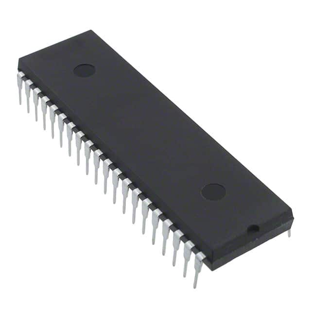
NXP Semiconductors SC16C650BIN40,112
- Part No.:
- SC16C650BIN40,112
- Manufacturer:
- NXP Semiconductors
- Package:
- 40-DIP (0.600", 15.24mm)
- Datasheet:
-
 SC16C650BIN40,112.pdf
- Description:
- IC UART SINGLE W/FIFO 40-DIP
- Quantity:
- Payment:

- Shipping:

Inventory:1,585
Please send an inquiry. Send us your inquiry, and we will respond immediately.
Product details
Overview
SC16C650BIN40 from NXP Semiconductors (formerly Philips) is a single-channel UART IC for asynchronous serial communication, converting parallel CPU data to serial streams and vice versa. It supports 5 V / 3.3 V / 2.5 V operation, delivers up to 3 Mbit/s at 5 V, integrates 32-byte TX/RX FIFOs, and includes IrDA 1.0 encoder/decoder for infrared data links - used in industrial terminal interfaces, legacy PC add-in cards, and embedded modem subsystems.
For engineers reviewing the SC16C650BIN40 datasheet, SC16C650BIN40 pinout, SC16C650BIN40 application, or SC16C650BIN40 equivalent, key selection criteria include FIFO trigger level programmability, auto-RTS/CTS hardware flow control implementation, IrDA 115.2 kbit/s support, and DIP40 package compatibility with legacy ISA bus designs.
Technical Context
The SC16C650BIN40 implements a dual-FIFO architecture with independent 32-byte transmit and receive buffers, four selectable interrupt trigger levels per FIFO, and time-out detection on RX to prevent data loss during CPU latency. Its baud rate generator accepts up to 48 MHz input clock and divides by configurable 16-bit divisor (DLL/DLM), enabling precise rates from DC to 3 Mbit/s.
Hardware flow control operates via dedicated CTS (input) and RTS (output) pins with auto-CTS mode halting transmission on CTS deassertion, and auto-RTS mode dynamically asserting RTS when RX FIFO reaches programmed threshold. Internal register mapping follows 16C450 compatibility on power-up, with enhanced features (EFR, Xon/Xoff registers) accessible only after LCR[7] = 1.
Key Specifications
| Parameter | Value and Actual Design Meaning |
|---|---|
| Supply Voltage | 2.5 V / 3.3 V / 5 V ±10% - supports mixed-voltage system integration without level shifters. |
| Max Data Rate | 3 Mbit/s at 5 V (48 MHz clock); 2 Mbit/s at 3.3 V; 1 Mbit/s at 2.5 V - enables high-speed modem and networking interfaces. |
| FIFO Depth | 32-byte TX + 32-byte RX - reduces CPU interrupt load by >60% vs. 16C550 (16-byte FIFO) in burst-mode transfers. |
| IrDA Support | IrDA 1.0 physical layer (115.2 kbit/s) - enables bidirectional infrared communication without external encoder/decoder ICs. |
| Interrupt Architecture | Prioritized, maskable interrupts for RX/TX/data-ready, line status, modem status, and flow control events - allows deterministic real-time response in multitask OS environments. |
| Operating Temperature | −40 °C to +85 °C - qualified for industrial control panels, factory automation, and outdoor telecom equipment. |
| Crystal Input | XTAL1/XTAL2 supports parallel-resonant crystals (e.g., 1.8432 MHz, 22–33 pF load) or external clock source - simplifies timing design across platforms. |
Pinout & Package
SC16C650BIN40 is housed in a 40-pin plastic dual in-line package (DIP40, 600 mil width, SOT129-1), compatible with through-hole PCB assembly and legacy ISA bus socket footprints.
| Pin/Terminal | Circuit Role | Design Meaning |
|---|---|---|
| D0–D7 | Data Bus I/O | 8-bit bidirectional TTL-compatible interface to CPU data bus; 3-state outputs enable shared bus arbitration. |
| A0–A2 | Register Address | Selects internal UART register (THR, LSR, MCR, etc.) during read/write cycles; decoded with CS0–CS2 and AS. |
| TX / RX | Serial I/O | Asynchronous serial output (TX) and input (RX) with start/stop/parity framing; supports RS-232/RS-485 transceivers. |
| RTS / CTS | Flow Control | Hardware handshaking signals: RTS output asserts when RX FIFO nears threshold; CTS input suspends TX on deassertion. |
| INT | Interrupt Output | Active-high open-drain interrupt signal indicating pending RX/TX/modem/line-status event; prioritized and maskable. |
| RESET | Master Reset | Active-high asynchronous reset initializing all registers to 16C450-compatible state and clearing FIFOs. |
| XTAL1 / XTAL2 | Oscillator Interface | Connects to crystal (1.8432 MHz typical) or external clock; XTAL2 floats in sleep mode to reduce power. |
| RCLK | Receiver Clock | Optional 16× baud-rate clock input for receiver section - allows independent TX/RX clocking in custom timing schemes. |
Key Features
| Feature | Design Value |
|---|---|
| Auto-RTS/CTS Flow Control | Reduces software overhead by automating RTS assertion based on RX FIFO fill level and halting TX on CTS deassertion - critical for real-time data acquisition systems. |
| Programmable FIFO Trigger Levels | Four selectable thresholds (8/16/24/28 bytes) per FIFO - enables fine-grained trade-off between interrupt frequency and latency in embedded Linux or RTOS drivers. |
| IrDA Encoder/Decoder | Integrated 115.2 kbit/s infrared PHY compliant with IrDA 1.0 - eliminates need for discrete IR transceiver, saving board space and BOM cost in handheld diagnostics tools. |
| Sleep Mode | Reduces current draw by disabling oscillator and internal logic while retaining register state - extends battery life in portable industrial scanners. |
| 16C450 Software Compatibility | Power-on default register map matches 16C450; runs unmodified DOS/Windows legacy UART drivers - ensures drop-in replacement in aging infrastructure. |
Applications
| Industrial HMI Terminal | Legacy PC Expansion Card |
|---|---|
|
Use Scenario: Serial communication between PLC and operator panel using RS-232 with variable baud rates and noise-prone factory floor cabling. IC Role / Device Role / Timing Role: UART interface IC handling protocol framing, FIFO buffering, and hardware flow control to prevent buffer overrun during rapid button-press bursts. Use Value: 32-byte FIFOs absorb transient data spikes; auto-RTS/CTS adapts to changing cable lengths and EMI conditions without driver reconfiguration. |
Use Scenario: ISA-bus serial port card adding COM3/COM4 to vintage industrial PCs running Windows NT or DOS-based SCADA software. IC Role / Device Role / Timing Role: Drop-in 16C450-compatible UART providing backward-compatible register access while delivering higher throughput for modem/fax applications. Use Value: DIP40 package fits standard ISA socket footprint; 5 V operation and 16C450 software compatibility ensure zero firmware changes during upgrade. |
| Embedded Modem Subsystem | Infrared Diagnostic Tool |
|
Use Scenario: High-speed data pump in DSL/cable modem bridging between DSP engine and analog front-end, requiring reliable flow-controlled serial link. IC Role / Device Role / Timing Role: Asynchronous data converter with DMA-ready signaling (TXRDY/RXRDY) and programmable baud generation for adaptive line rates. Use Value: 3 Mbit/s capability supports V.34/V.90 modem standards; independent TX/RX trigger levels optimize throughput in asymmetric upload/download scenarios. |
Use Scenario: Handheld field service tool communicating with HVAC controllers or energy meters via infrared link in environments where RF is prohibited. IC Role / Device Role / Timing Role: Integrated IrDA 1.0 PHY encoder/decoder eliminating external transceiver; UART handles packetization and error checking. Use Value: On-chip IrDA reduces component count by 3+ parts; sleep mode cuts quiescent current to <100 µA for multi-year battery life. |
Equivalent & Alternatives
The following parts are listed as comparable options for similar UART applications.
| Alternative Part | Technical Difference | Application Difference | Selection Advice |
|---|---|---|---|
| TL16C650CPTR | TI part with identical 32-byte FIFOs, IrDA 1.0, and 5 V operation but requires external 3.3 V regulator for 3.3 V logic interface; no 2.5 V support. | Best suited for new 5 V-only designs where TI supply chain preference applies; not pin-compatible due to different pin 1 location and CS pin assignment. | Select TL16C650CPTR only if migrating from TI ecosystem and accepting layout revision for CS pin routing and voltage regulation. |
| ST16C654CJ44 | 4-channel variant in PLCC44; shares same register set and FIFO architecture but adds three additional UARTs and different interrupt multiplexing logic. | Used in multi-port serial servers or PCI express serial cards where channel density outweighs single-channel cost efficiency. | Choose ST16C654CJ44 when expanding to ≥4 serial ports on one board; avoid for single-port replacements due to non-equivalent pinout and package mismatch. |
Compared with TL16C650CPTR and ST16C654CJ44, the SC16C650BIN40 uniquely combines DIP40 through-hole packaging, triple-voltage operation (2.5/3.3/5 V), and full 16C450 software compatibility - making it the sole option for drop-in upgrades of legacy industrial hardware without PCB redesign.
Availability
SC16C650BIN40 is available at Aetrix Electronics and suitable for industrial HMI terminals, legacy PC expansion cards, embedded modem subsystems, and infrared diagnostic tools requiring stable component supply across extended product lifecycles.
Supply support for SC16C650BIN40 includes scheduled delivery planning, volume procurement assistance, BOM continuity management, traceable sourcing, and lifecycle availability coordination for OEM customers, industrial embedded developers, connected-device designers, and electronics production programs.
Manufacturer
NXP Semiconductors, formerly Philips Semiconductors, is a global leader in high-performance mixed-signal ICs for automotive, industrial, and communication markets, with deep expertise in legacy interface solutions.
The SC16C650BIN40 belongs to NXP's industrial UART product line, designed specifically to extend the service life of aging serial infrastructure while adding modern features like IrDA and multi-voltage operation.
FAQ
What voltage levels does the SC16C650BIN40 support, and how does that affect system design?
The SC16C650BIN40 operates at 2.5 V, 3.3 V, or 5 V ±10%, with 5 V-tolerant inputs. This allows direct interfacing with legacy 5 V microcontrollers, modern 3.3 V FPGAs, or low-power 2.5 V SoCs without external level shifters. The SC16C650BIN40 maintains full functionality-including 3 Mbit/s operation and IrDA encoding-at all three voltages, simplifying mixed-voltage board design and reducing BOM count.
How does the SC16C650BIN40 handle hardware flow control, and what are the configuration requirements?
The SC16C650BIN40 implements auto-RTS and auto-CTS via dedicated pins and internal logic controlled by the Enhanced Feature Register (EFR). Auto-CTS halts transmission when CTS goes inactive; auto-RTS asserts RTS when RX FIFO reaches a user-programmed trigger level (8/16/24/28 bytes). To enable either function, EFR[6] (RTS) or EFR[7] (CTS) must be set to 1, and the UART must be in enhanced mode (LCR[7] = 1). The SC16C650BIN40 requires no external logic to implement robust hardware handshaking.
Can the SC16C650BIN40 replace a standard 16C450 UART without firmware changes?
Yes - the SC16C650BIN40 powers up in 16C450-compatible mode: all registers match the 16C450 map, and default settings (e.g., 1-stop bit, no parity, 8-bit words) align with legacy drivers. Existing DOS, Windows NT, or embedded OS UART drivers run unchanged. Advanced features like FIFOs and IrDA remain disabled until explicitly enabled via register writes, ensuring seamless integration into deployed systems.
What is the maximum data rate achievable with the SC16C650BIN40, and what clock frequency is required?
The SC16C650BIN40 achieves up to 3 Mbit/s at 5 V using a 48 MHz input clock (XTAL1), as the internal baud generator divides this 16× clock by a programmable 16-bit divisor. At 3.3 V, max rate drops to 2 Mbit/s; at 2.5 V, to 1 Mbit/s. For standard rates like 115.2 kbit/s, a 1.8432 MHz crystal suffices. The SC16C650BIN40's BAUDOUT pin provides the 16× clock for external receivers or transceivers.
Does the SC16C650BIN40 support infrared communication, and what IrDA version is implemented?
Yes - the SC16C650BIN40 integrates a full IrDA 1.0 physical layer encoder/decoder supporting up to 115.2 kbit/s. It handles pulse shaping, RZI modulation, and 3/16 pulse width encoding per IrDA spec, eliminating need for external IR transceivers. The SC16C650BIN40 uses standard UART registers to configure IrDA mode, and its DIP40 package allows direct connection to IR LED/detector arrays in compact diagnostic tools.
SC16C650BIN40,112 Specifications
- Product attributes
- Attribute value
- Manufacturer:
- NXP Semiconductors
- Package/Case:
- 40-DIP (0.600", 15.24mm)
- Series:
- -
- Packaging:
- Tube
- Product Status:
- Obsolete
- Features:
- -
- Number of Channels:
- 1, UART
- FIFO's:
- 32 Byte
- Protocol:
- -
- Data Rate (Max):
- 3Mbps
- Voltage - Supply:
- 2.5V, 3.3V, 5V
- With Auto Flow Control:
- Yes
- With IrDA Encoder/Decoder:
- Yes
- With False Start Bit Detection:
- Yes
- With Modem Control:
- Yes
- Grade:
- -
- Qualification:
- -
- Mounting Type:
- Through Hole
- Supplier Device Package:
- 40-DIP
SC16C650BIN40,112 FAQ
1.How can I place an order for SC16C650BIN40,112 through Aetrix?
Please submit a Request for Quotation (RFQ) for SC16C650BIN40,112 on Aetrix. Our sales agent will provide a competitive quotation and guide you through the order confirmation once you accept the terms.
2.Are the price and stock information for SC16C650BIN40,112 reliable?
The price and inventory of SC16C650BIN40,112 are updated periodically and may fluctuate due to market conditions. Stock and pricing data are typically refreshed every 24 hours. Quotation validity for SC16C650BIN40,112 is usually 5 days.
3.What payment methods are accepted for SC16C650BIN40,112?
We accept Wire Transfer, PayPal, Credit Card, Western Union, MoneyGram, and Escrow for SC16C650BIN40,112 transactions.
Note: Certain payment methods may incur a processing fee.
4.How is shipping managed for SC16C650BIN40,112?
SC16C650BIN40,112 orders can be shipped via leading logistics carriers, including DHL, UPS, FedEx, TNT, or Registered Mail.
Once your SC16C650BIN40,112 order is processed, you will receive an email with the shipment details and tracking number.
Note: Tracking information may take up to 24 hours to appear. Express delivery typically takes 3–5 business days.
5.How can I obtain technical support or documentation for SC16C650BIN40,112?
For technical support, including SC16C650BIN40,112 datasheets, pinout diagrams, or application guidance, please contact our engineering support team. They can provide detailed documentation and assistance for your SC16C650BIN40,112 requirements.
6.How does Aetrix verify that SC16C650BIN40,112 is sourced from the original manufacturer or authorized distributors?
All SC16C650BIN40,112 products on Aetrix are procured from qualified distributors and authorized channels. Our dedicated quality assurance team conducts strict verification, including traceability checks and, if necessary, third-party testing. This ensures that SC16C650BIN40,112 meets industry standards.
7.What is the process for return or replacement of SC16C650BIN40,112?
All SC16C650BIN40,112 units undergo pre-shipment inspection (PSI). If there is an issue with SC16C650BIN40,112, returns or replacements are accepted under the following conditions:
1.Quantity discrepancies, incorrect items, or visible external defects (such as breakage or corrosion), acknowledged by Aetrix.
2.The issue is reported within 90 days of delivery.
3.The SC16C650BIN40,112 part is unused and in its original packaging.
Return procedure for SC16C650BIN40,112:
1.Submit a request within 90 days.
2.Obtain a Return Material Authorization (RMA) from Aetrix.
SC16C650BIN40,112 Tags

-
SC16IS741AIPWJ
NXP Semiconductors

-
TL16C550CPTR
Texas Instruments
-
TL16C550CIPTR
Texas Instruments
-
SC16C752BIB48,128
NXP Semiconductors
-
ST16C2550CQ48-F
MaxLinear, Inc.
-
ST16C2550CJ44-F
MaxLinear, Inc.
-
ST16C2552CJ44-F
MaxLinear, Inc.
-
ST16C1550IQ48-F
MaxLinear, Inc.
-
ST16C2550IQ48-F
MaxLinear, Inc.

-
ST16C554DIQ64-F
MaxLinear, Inc.
-
ST16C554DCQ64-F
MaxLinear, Inc.
-
XR17V352IB113-F
MaxLinear, Inc.
Tech Hub

A practical engineering guide to 3.3V and 5V logic compatibility, input thresholds, resistor dividers, translator ICs, MOSFET level shifting, I2C pull-ups, timing limits and power-sequencing risks.

The 74HC595 uses push-pull logic outputs, while the TPIC6B595 uses 50 V open-drain DMOS sinks for higher-power loads. This guide compares timing, current limits, 3.3 V interfacing, load wiring, thermal…

The 74HC595 converts serial data into eight stable parallel outputs. This guide covers pin functions, shift and storage timing, OE and MR behavior, drive-current limits, cascading, voltage compatibilit…

A technical comparison of level-sensitive latches and edge-triggered flip-flops, covering timing windows, setup and hold limits, master–slave operation, time borrowing, race-through, HDL inference and…

A D latch stores one bit while Enable controls when data can pass. This reference covers gate-level operation, truth tables, transparency, setup and hold timing, LE versus OE, common ICs and practical …

An SR latch stores one bit through cross-coupled feedback. This engineering reference covers NOR and NAND implementations, truth tables, forbidden-state recovery, gated operation, switch debouncing, fa…

Latch circuits retain one bit through feedback. This technical reference covers SR and D latches, truth tables, transparency, timing limits, latch-versus-flip-flop behavior, applications and common log…

An engineering guide to LED driver operation, constant-current and constant-voltage outputs, linear and switching topologies, dimming, IC selection, calculations, replacement compatibility, and fault c…

Operational amplifier guide covering op amp basics, feedback, ideal vs real op amps, common configurations, buffer circuits, offset, bias current, gain-bandwidth, slew rate, rail-to-rail limits and sel…

Jumper cables guide covering safe connection order, red and black clamp placement, final ground connection, cable gauge, length, clamp quality, copper vs CCA cables, jump starter comparison and battery…


