
 My Inquiry
 My Account


NXP Semiconductors SC16C750IA44,512
.jpg)
- Part No.:
- SC16C750IA44,512
- Manufacturer:
- NXP Semiconductors
- Package:
- 44-LCC (J-Lead)
- Datasheet:
-
 SC16C750IA44,512.pdf
- Description:
- IC UART 64BYTE 44PLCC
- Quantity:
- Payment:

- Shipping:

Inventory:2,910
Please send an inquiry. Send us your inquiry, and we will respond immediately.
Product details
Overview
SC16C750IA44,512 from NXP Semiconductors (formerly Philips) is a 64-byte FIFO Universal Asynchronous Receiver/Transmitter (UART) IC for high-speed serial data conversion in embedded communication interfaces. It supports up to 3 Mbits/s at 5 V, features auto-RTS/CTS hardware flow control, 64-byte TX/RX FIFOs, and operates across 2.5 V, 3.3 V, and 5 V supply rails in industrial temperature range (−40 °C to +85 °C).
For engineers reviewing the SC16C750IA44,512 datasheet, SC16C750IA44,512 pinout, SC16C750IA44,512 application, or SC16C750IA44,512 equivalent, this device delivers deterministic interrupt latency, programmable FIFO trigger levels, DMA-ready signaling (TXRDY/RXRDY), and backward compatibility with 16C450/16C550 software stacks - critical for legacy system upgrades and multi-channel modem/data link designs.
Technical Context
The SC16C750IA44,512 implements a dual-FIFO architecture with independent 64-byte transmit and receive buffers, enabling burst-mode DMA transfers and reducing CPU polling overhead. Its enhanced feature register (EFR) enables automatic hardware flow control via RTS/CTS, with configurable trigger thresholds and time-out interrupts for reliable full-duplex operation.
It integrates a fully programmable baud rate generator accepting up to 48 MHz input clock, supporting standard and custom rates (e.g., 115.2 kbit/s, 460.8 kbit/s) via DLL/DLM divisor latches. Internal loop-back mode and sleep mode (activated via IER[4]) support on-board diagnostics and low-power idle states without external circuitry.
Key Specifications
| Parameter | Value and Actual Design Meaning |
|---|---|
| Max Data Rate | 3 Mbits/s at 5 V - enables direct interface with high-speed modems and ISDN controllers without external rate limiting. |
| FIFO Depth | 64-byte TX + 64-byte RX - reduces interrupt frequency by >95% vs. 16C450, allowing longer CPU task windows in real-time systems. |
| Supply Voltage | 2.5 V / 3.3 V / 5 V ±10% - supports mixed-voltage board designs and legacy 5 V backplanes alongside modern low-voltage logic. |
| Operating Temp | −40 °C to +85 °C - qualified for industrial automation, telecom infrastructure, and transportation control units. |
| Interrupt Priority | Four-level prioritized interrupt system - ensures timely handling of line status, receive data ready, transmit empty, and modem events. |
| Baud Generator | Divisor range 1–65535 - achieves exact standard rates (e.g., 9600, 115200) and custom rates (e.g., 460800) using 1.8432 MHz or 48 MHz clocks. |
| Flow Control | Programmable auto-RTS/CTS with four selectable RX trigger levels (1/4/8/14 chars) - eliminates software-based handshaking overhead in multi-drop networks. |
Pinout & Package
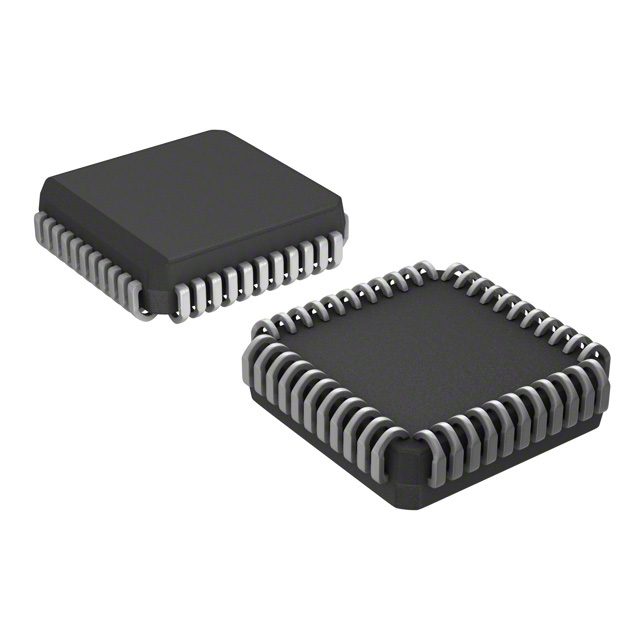
SC16C750IA44,512 is housed in a plastic leaded chip carrier (PLCC44) package with 44 leads, 1.27 mm pitch, and JEDEC MO-047A outline. Pin 1 is located at corner marked by notch or dot; pins are numbered counter-clockwise.
| Pin/Terminal | Circuit Role | Design Meaning |
|---|---|---|
| A0–A2 | Register Address Select | Selects internal UART register (THR/RHR, IER, FCR, LCR, etc.) during read/write cycles; required for full register access. |
| CS0–CS2 | Chip Select Inputs | Enable device when CS0=HIGH, CS1=HIGH, CS2=LOW; AS signal determines whether address strobe is active or latched. |
| IOR / IOW | Read/Write Control | Asymmetric active-low/high inputs - only one needed per cycle; allows flexible bus timing with 8080- or Z80-style microcontrollers. |
| TX / RX | Serial Data I/O | Full-duplex asynchronous data path; TX output drives RS-232/RS-422 transceivers; RX input accepts TTL/CMOS-level serial streams. |
| RTS / CTS | Hardware Flow Control | RTS output asserts when RX FIFO nears threshold; CTS input halts TX upon remote buffer full - enables zero-software flow management. |
| TXRDY / RXRDY | DMA Ready Signals | Active-low outputs indicate FIFO readiness for DMA transfer; support both single-cycle (mode 0) and burst (mode 1) DMA protocols. |
| INT | Interrupt Output | Open-drain HIGH-active interrupt; combines line status, data ready, modem change, and timeout events into one prioritized signal. |
| XTAL1 / XTAL2 | Crystal Oscillator Interface | Supports parallel-resonant crystal (1.8432–48 MHz) or external clock input; XTAL2 floats in sleep mode to reduce power. |
Key Features
| Feature | Design Value |
|---|---|
| 64-byte TX/RX FIFOs | Reduces CPU interrupt load by >80% vs. 16C550 in high-throughput applications such as multi-port terminal servers. |
| Auto-RTS/CTS Hardware Flow Control | Eliminates software polling of modem status bits; enables deterministic latency for real-time protocol stacks (e.g., PPP, HDLC). |
| Four Receive Interrupt Trigger Levels | Allows tuning of interrupt frequency to match host CPU bandwidth - e.g., 1-byte trigger for low-latency control links, 14-byte for bulk data. |
| Sleep Mode with Wake-on-Event | Reduces quiescent current to <100 µA; wakes on start bit, modem pin transition (RI/CTS/DSR), or TX data write - ideal for battery-backed systems. |
| Internal Loop-Back Diagnostics | Validates TX/RX path integrity without external cabling; supports automated production test and field firmware self-check routines. |
Applications
| Industrial PLC Communication Module | Legacy PC Serial Port Replacement |
|---|---|
|
Use Scenario: Serial interface between PLC CPU and RS-485 fieldbus gateway handling Modbus RTU traffic at 115.2 kbit/s. IC Role / Device Role / Timing Role: UART bridge converting parallel bus data to framed asynchronous serial stream with precise framing (start/stop/parity) and error detection. Use Value: 64-byte FIFO absorbs bursty sensor data bursts; auto-CTS prevents overrun during network congestion; industrial temp rating ensures reliability in cabinet environments. |
Use Scenario: Drop-in upgrade of ISA/PCI serial cards replacing obsolete 16C550 chips in medical diagnostic equipment requiring FDA-compliant firmware reuse. IC Role / Device Role / Timing Role: Pin-compatible UART providing identical register map and interrupt behavior to 16C450, enabling zero-modification driver reuse. Use Value: Backward software compatibility preserves certified OS drivers; 3.3 V operation reduces heat in dense card stacks; PLCC44 footprint matches legacy layouts. |
| Multi-Channel Modem Data Concentrator | Embedded Linux Terminal Server |
|
Use Scenario: 8-port V.34 modem bank aggregating dial-up connections for remote site telemetry, with each port running at 33.6 kbit/s. IC Role / Device Role / Timing Role: High-speed UART with independent baud rate generation per channel, synchronized to shared 48 MHz clock. Use Value: 3 Mbit/s capability supports compressed modem rates; programmable TX/RX FIFO triggers prevent inter-channel interference; DMA signaling offloads ARM9 host CPU. |
Use Scenario: ARM-based edge gateway running OpenWrt, managing console access over USB-to-serial adapters and local debug ports. IC Role / Device Role / Timing Role: Primary UART controller for kernel console and bootloader serial I/O, configured for 115200-N-8-1 with hardware flow control. Use Value: Sleep mode extends uptime in solar-powered deployments; false start-bit detection improves noise immunity on long cables; loop-back mode enables field firmware validation. |
Equivalent & Alternatives
The following parts are listed as comparable options for similar UART applications.
| Alternative Part | Technical Difference | Application Difference | Selection Advice |
|---|---|---|---|
| SC16C752IB64 | Same core UART but in LQFP64 package with additional DTR/RI/DCD/DSR pins exposed; no PLCC44 footprint. | Used where board space permits larger QFP and full modem pinout is required (e.g., standalone modem design). | Select SC16C752IB64 only if LQFP64 layout and extended modem signaling are needed; not pin-compatible with SC16C750IA44,512. |
| TI TL16C750IPM | Pin-compatible 64-byte FIFO UART but rated only for 5 V operation; lacks 2.5 V/3.3 V support and sleep mode. | Suitable for legacy 5 V-only systems where low-power operation is not required and voltage scaling is unnecessary. | Choose TL16C750IPM only for cost-sensitive 5 V designs without mixed-voltage or ultra-low-power requirements. |
Compared with SC16C750IA44,512, the SC16C752IB64 offers expanded modem I/O in a different package, while the TL16C750IPM provides functional equivalence only at 5 V without sleep or multi-voltage capability - making SC16C750IA44,512 uniquely suited for industrial mixed-voltage and power-constrained applications.
Availability
SC16C750IA44,512 is available at Aetrix Electronics and suitable for industrial PLC communication modules, legacy PC serial port replacements, multi-channel modem concentrators, and embedded Linux terminal servers requiring stable component supply across extended product lifecycles.
Supply support for SC16C750IA44,512 includes scheduled delivery planning, volume procurement assistance, BOM continuity management, traceable sourcing, and lifecycle availability coordination for OEM customers, industrial embedded developers, connected-device designers, and electronics production programs.
Manufacturer
NXP Semiconductors (originally Philips Semiconductors) is a global leader in high-performance mixed-signal ICs, with expertise in connectivity, security, and automotive electronics.
The SC16C750IA44,512 belongs to NXP's legacy UART product line, designed specifically for robust, drop-in replacement of 16C450/16C550 in industrial and telecom infrastructure where reliability, wide voltage operation, and deterministic interrupt response are mandatory.
FAQ
What is the maximum serial data rate supported by the SC16C750IA44,512?
The SC16C750IA44,512 supports up to 3 Mbits/s at 5 V supply, 2 Mbits/s at 3.3 V, and 1 Mbit/s at 2.5 V. This is achieved using a 48 MHz external clock input divided by the programmable baud rate generator. The actual achievable rate depends on crystal accuracy, PCB layout, and transceiver drive strength - verified in the SC16C750IA44,512 datasheet Rev. 04, Section 6.5.
Does the SC16C750IA44,512 support automatic hardware flow control?
Yes, the SC16C750IA44,512 supports automatic hardware flow control via RTS/CTS signals. When enabled through the Enhanced Feature Register (EFR), it automatically asserts RTS based on RX FIFO fill level and suspends transmission when CTS is deasserted. This behavior is fully documented in Section 6.3 of the SC16C750IA44,512 product data sheet.
Is the SC16C750IA44,512 pin-compatible with older UARTs like the 16C450?
Yes, the SC16C750IA44,512 powers up functionally equivalent to the 16C450 and maintains pin compatibility with TL16C750 and ST16C450/550 families. Its PLCC44 footprint and signal mapping match industry-standard layouts, enabling direct replacement without PCB changes - confirmed in Section 1 and Table 1 of the SC16C750IA44,512 datasheet.
How does the sleep mode operate in the SC16C750IA44,512?
The SC16C750IA44,512 enters sleep mode when IER[4] is set, reducing current draw to under 100 µA. It wakes automatically on start-bit detection, modem pin transitions (RI/CTS/DSR/DCD), or TX data write. After servicing the wake event, it re-enters sleep unless interrupts remain pending - detailed in Section 6.7 of the SC16C750IA44,512 product data.
Can the SC16C750IA44,512 be used with a 1.8432 MHz crystal?
Yes, the SC16C750IA44,512 supports 1.8432 MHz crystals for standard baud rates (e.g., 9600, 19200, 115200). Table 5 in the SC16C750IA44,512 datasheet lists exact divisor values and error margins. The crystal connects between XTAL1 and XTAL2 pins with recommended 22 pF/47 pF load capacitors per Figure 4.
SC16C750IA44,512 Specifications
- Product attributes
- Attribute value
- Manufacturer:
- NXP Semiconductors
- Package/Case:
- 44-LCC (J-Lead)
- Series:
- -
- Packaging:
- Tube
- Product Status:
- Obsolete
- Features:
- -
- Number of Channels:
- 1, UART
- FIFO's:
- 64 Byte
- Protocol:
- -
- Data Rate (Max):
- 3Mbps
- Voltage - Supply:
- 2.5V, 3.3V, 5V
- With Auto Flow Control:
- Yes
- With IrDA Encoder/Decoder:
- -
- With False Start Bit Detection:
- Yes
- With Modem Control:
- Yes
- Grade:
- -
- Qualification:
- -
- Mounting Type:
- Surface Mount
- Supplier Device Package:
- 44-PLCC (16.59x16.59)
SC16C750IA44,512 FAQ
1.How can I place an order for SC16C750IA44,512 through Aetrix?
Please submit a Request for Quotation (RFQ) for SC16C750IA44,512 on Aetrix. Our sales agent will provide a competitive quotation and guide you through the order confirmation once you accept the terms.
2.Are the price and stock information for SC16C750IA44,512 reliable?
The price and inventory of SC16C750IA44,512 are updated periodically and may fluctuate due to market conditions. Stock and pricing data are typically refreshed every 24 hours. Quotation validity for SC16C750IA44,512 is usually 5 days.
3.What payment methods are accepted for SC16C750IA44,512?
We accept Wire Transfer, PayPal, Credit Card, Western Union, MoneyGram, and Escrow for SC16C750IA44,512 transactions.
Note: Certain payment methods may incur a processing fee.
4.How is shipping managed for SC16C750IA44,512?
SC16C750IA44,512 orders can be shipped via leading logistics carriers, including DHL, UPS, FedEx, TNT, or Registered Mail.
Once your SC16C750IA44,512 order is processed, you will receive an email with the shipment details and tracking number.
Note: Tracking information may take up to 24 hours to appear. Express delivery typically takes 3–5 business days.
5.How can I obtain technical support or documentation for SC16C750IA44,512?
For technical support, including SC16C750IA44,512 datasheets, pinout diagrams, or application guidance, please contact our engineering support team. They can provide detailed documentation and assistance for your SC16C750IA44,512 requirements.
6.How does Aetrix verify that SC16C750IA44,512 is sourced from the original manufacturer or authorized distributors?
All SC16C750IA44,512 products on Aetrix are procured from qualified distributors and authorized channels. Our dedicated quality assurance team conducts strict verification, including traceability checks and, if necessary, third-party testing. This ensures that SC16C750IA44,512 meets industry standards.
7.What is the process for return or replacement of SC16C750IA44,512?
All SC16C750IA44,512 units undergo pre-shipment inspection (PSI). If there is an issue with SC16C750IA44,512, returns or replacements are accepted under the following conditions:
1.Quantity discrepancies, incorrect items, or visible external defects (such as breakage or corrosion), acknowledged by Aetrix.
2.The issue is reported within 90 days of delivery.
3.The SC16C750IA44,512 part is unused and in its original packaging.
Return procedure for SC16C750IA44,512:
1.Submit a request within 90 days.
2.Obtain a Return Material Authorization (RMA) from Aetrix.
SC16C750IA44,512 Tags

-
SC16IS741AIPWJ
NXP Semiconductors

-
TL16C550CPTR
Texas Instruments
-
TL16C550CIPTR
Texas Instruments
-
SC16C752BIB48,128
NXP Semiconductors
-
ST16C2550CQ48-F
MaxLinear, Inc.
-
ST16C2550CJ44-F
MaxLinear, Inc.
-
ST16C2552CJ44-F
MaxLinear, Inc.
-
ST16C1550IQ48-F
MaxLinear, Inc.
-
ST16C2550IQ48-F
MaxLinear, Inc.

-
ST16C554DIQ64-F
MaxLinear, Inc.
-
ST16C554DCQ64-F
MaxLinear, Inc.
-
XR17V352IB113-F
MaxLinear, Inc.
Tech Hub

A practical engineering guide to 3.3V and 5V logic compatibility, input thresholds, resistor dividers, translator ICs, MOSFET level shifting, I2C pull-ups, timing limits and power-sequencing risks.

The 74HC595 uses push-pull logic outputs, while the TPIC6B595 uses 50 V open-drain DMOS sinks for higher-power loads. This guide compares timing, current limits, 3.3 V interfacing, load wiring, thermal…

The 74HC595 converts serial data into eight stable parallel outputs. This guide covers pin functions, shift and storage timing, OE and MR behavior, drive-current limits, cascading, voltage compatibilit…

A technical comparison of level-sensitive latches and edge-triggered flip-flops, covering timing windows, setup and hold limits, master–slave operation, time borrowing, race-through, HDL inference and…

A D latch stores one bit while Enable controls when data can pass. This reference covers gate-level operation, truth tables, transparency, setup and hold timing, LE versus OE, common ICs and practical …

An SR latch stores one bit through cross-coupled feedback. This engineering reference covers NOR and NAND implementations, truth tables, forbidden-state recovery, gated operation, switch debouncing, fa…

Latch circuits retain one bit through feedback. This technical reference covers SR and D latches, truth tables, transparency, timing limits, latch-versus-flip-flop behavior, applications and common log…

An engineering guide to LED driver operation, constant-current and constant-voltage outputs, linear and switching topologies, dimming, IC selection, calculations, replacement compatibility, and fault c…

Operational amplifier guide covering op amp basics, feedback, ideal vs real op amps, common configurations, buffer circuits, offset, bias current, gain-bandwidth, slew rate, rail-to-rail limits and sel…

Jumper cables guide covering safe connection order, red and black clamp placement, final ground connection, cable gauge, length, clamp quality, copper vs CCA cables, jump starter comparison and battery…


