
 My Inquiry
 My Account


NXP Semiconductors SC26C92C1B,528
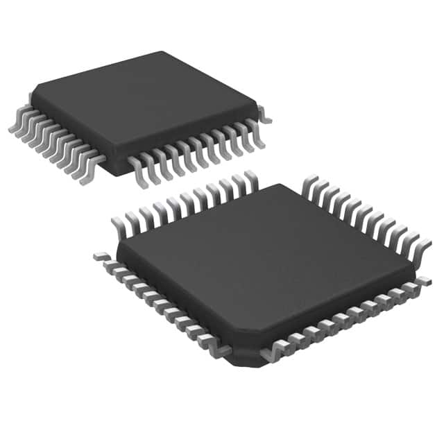
- Part No.:
- SC26C92C1B,528
- Manufacturer:
- NXP Semiconductors
- Package:
- 44-QFP
- Datasheet:
-
 SC26C92C1B,528.pdf
- Description:
- IC UART DUAL W/FIFO 44QFP
- Quantity:
- Payment:

- Shipping:

Inventory:4,669
Please send an inquiry. Send us your inquiry, and we will respond immediately.
Product details
Overview
SC26C92C1B,528 from NXP Semiconductors (formerly Philips) is a dual-channel CMOS universal asynchronous receiver/transmitter (DUART) in 44-pin PQFP package, supporting independent full-duplex serial communication on two channels with 8-character FIFOs per channel, programmable baud rates up to 230.4 kbaud, and single +5 V supply. It serves as a pin- and function-compatible upgrade to SCC2692 and SCN2681 in industrial terminal controllers, legacy industrial PLCs, and multi-drop RS-232/RS-485 systems.
For engineers reviewing the SC26C92C1B,528 datasheet, SC26C92C1B,528 pinout, SC26C92C1B,528 application, or SC26C92C1B,528 equivalent, key selection considerations include its dual-channel independent baud rate configuration, 8-byte FIFO depth per channel, watchdog timer per receiver, programmable counter/timer for custom clock generation, and support for multidrop wake-up mode - all critical for deterministic serial interface design in embedded control systems.
Technical Context
The SC26C92C1B,528 implements two independent UART channels (A and B), each with dedicated 8-character transmit and receive FIFOs, separate baud rate generators, and configurable interrupt sources. Its timing subsystem integrates an on-chip crystal oscillator (3.6864 MHz nominal), a 16-bit programmable counter/timer, and four clock selectors enabling independent 1X/16X clock routing to each receiver and transmitter.
It features a multipurpose 7-bit input port (IP0–IP6) with change-of-state detection on four pins and an 8-bit output port (OP0–OP7) supporting general-purpose I/O, modem control signals (RTS/CTS), and discrete interrupt outputs (e.g., RxRDY, TxRDY). The interrupt system provides one active-low open-drain INTRN output plus up to six wire-ORable outputs via OP3–OP7 when configured as interrupts.
Key Specifications
| Parameter | Value and Actual Design Meaning |
|---|---|
| Baud Rate Range | 50 to 230.4 kbaud; supports 27 fixed rates, external 1X/16X clocks, or user-defined rates via 16-bit counter/timer - enables precise synchronization with legacy host systems. |
| FIFO Depth | 8 characters per receiver and transmitter; reduces CPU interrupt overhead and prevents overrun/underrun in burst-mode serial traffic. |
| Supply Voltage | +5 V ±10%; operates across industrial temperature range (–40°C to +85°C) without level-shifting - simplifies integration into existing 5 V logic systems. |
| Package | 44-pin plastic quad flat pack (PQFP), SOT307-2; surface-mount compatible with standard reflow profiles and IPC-compliant board layouts. |
| Interrupt Architecture | Single INTRN output with eight maskable conditions plus six optional discrete interrupt outputs (OP3–OP7); allows flexible prioritization and hardware-level flow control signaling. |
| Receiver Watchdog Timer | Dedicated timer per channel detects idle line conditions and triggers timeout interrupt - essential for robust multidrop bus arbitration and fault recovery. |
| Data Format Flexibility | 5–8 data bits, 1/1.5/2 stop bits (in 1/16-bit increments), odd/even/no/force parity - ensures interoperability with diverse legacy protocols including IBM 3270, DEC VT100, and proprietary telemetry formats. |
Pinout & Package
SC26C92C1B,528 is housed in a 44-pin plastic quad flat pack (PQFP), SOT307-2, with 0.8 mm lead pitch and exposed thermal pad (non-electrical). Pin 1 is located at top-left corner with index mark; pin numbering proceeds counterclockwise.
| Pin/Terminal | Circuit Role | Design Meaning |
|---|---|---|
| 1–4, 42–44 | A3, IP0, WRN, RDN, A0–A2, VCC | Address/data control and power: A0–A3 select internal registers; WRN/RDN enable register access; VCC supplies +5 V core logic. |
| 5–6, 29–30 | RxDB, TxDB, RxDA, TxDA | Dual UART serial I/O: independent full-duplex channels A and B; TTL-level inputs/outputs compatible with standard line drivers. |
| 7–10, 24–27 | OP1–OP7, INTRN, OP0 | Programmable I/O and interrupt: OP0/OP1 serve as RTS outputs; OP2–OP7 configurable as clock outputs or open-drain interrupt signals (RxRDY, TxRDY, etc.). |
| 11, 16–17, 31–32 | NC, GND, RESET, X2 | Ground, reset, and crystal interface: GND pins provide low-impedance return; RESET initializes registers and disables transmitters; X1/CLK and X2 connect to 3.6864 MHz crystal. |
| 12–15, 18–23, 33–41 | D0–D7, IP2–IP6, CEN, X1/CLK | System interface: D0–D7 form bidirectional 8-bit data bus; CEN enables bus access; IP2–IP6 support external clocking, CTS, and counter/timer inputs; X1/CLK accepts crystal or external clock. |
Key Features
| Feature | Design Value |
|---|---|
| Dual independent UART channels | Enables simultaneous serial communication with two peripherals (e.g., modem + printer) without CPU time-slicing or external multiplexing. |
| 8-character FIFO per channel | Reduces interrupt frequency by >80% vs. single-character buffering - critical for real-time response in interrupt-driven firmware. |
| Programmable counter/timer | Generates precise 16X baud clocks or timeout intervals; eliminates need for external timing ICs in custom protocol implementations. |
| Automatic wake-up mode | Supports 9-bit multidrop addressing with address-match detection - allows selective activation of remote nodes on shared RS-485 buses. |
| RTS/CTS flow control | Hardware handshaking via OP0/OP1 (RTSA/RTSB) and IP0/IP1 (CTSA/CTSB) prevents buffer overflow without software polling. |
| On-chip crystal oscillator | Eliminates external oscillator components; supports 2–4 MHz crystals - reduces BOM cost and PCB area in space-constrained designs. |
Applications
| Industrial Terminal Controller | Legacy PLC Serial Interface |
|---|---|
|
Use Scenario: Connecting ASCII terminals, barcode scanners, and operator panels to a central controller via RS-232. IC Role / Device Role / Timing Role: Dual UART handles concurrent keyboard input (Channel A) and display output (Channel B) with independent baud rates and flow control. Use Value: 8-byte FIFOs prevent character loss during high-speed scanning bursts; watchdog timers detect disconnected peripherals and trigger fail-safe recovery. |
Use Scenario: Interfacing programmable logic controllers with HMI panels, motor drives, and sensor networks using RS-485 multidrop topology. IC Role / Device Role / Timing Role: DUART acts as master node UART with automatic wake-up mode to selectively activate slave devices on shared bus. Use Value: Multidrop mode (9-bit) and RTS/CTS signaling ensure reliable command delivery and status reporting across noisy factory-floor environments. |
| Point-of-Sale (POS) System Backplane | Medical Device Diagnostic Port |
|
Use Scenario: Integrating receipt printers, cash drawers, and magnetic stripe readers into a unified retail terminal chassis. IC Role / Device Role / Timing Role: SC26C92C1B,528 provides isolated serial paths for each peripheral with independent interrupt lines routed to microcontroller GPIOs. Use Value: Programmable output port (OP0–OP7) directly drives cash drawer solenoids and printer ready signals - eliminating discrete driver ICs. |
Use Scenario: Enabling service technicians to download firmware updates and retrieve diagnostic logs from patient monitors and infusion pumps. IC Role / Device Role / Timing Role: UART Channel A handles secure bootloader communication; Channel B supports real-time telemetry streaming over RS-232. Use Value: Receiver timeout mode detects cable disconnects or device resets; parity/framing error detection ensures integrity of critical calibration data transfers. |
Equivalent & Alternatives
The following parts are listed as comparable options for similar dual UART applications.
| Alternative Part | Technical Difference | Application Difference | Selection Advice |
|---|---|---|---|
| SC26C92A1B | Industrial-grade version (-40°C to +85°C) with identical pinout, functionality, and electrical specs; differs only in screening and test conditions. | Required for deployments outside commercial temperature range; suitable for outdoor kiosks or vehicle-mounted systems. | Select SC26C92A1B when operating ambient exceeds 70°C or requires extended reliability validation. |
| SCN2681C1B | Predecessor with 1-character FIFOs, no watchdog timer, no counter/timer, and limited baud rate flexibility (no programmable C/T-derived rates). | Lacks multidrop wake-up, flow control automation, and deep buffering - insufficient for high-throughput or fault-tolerant designs. | SC26C92C1B,528 offers direct functional upgrade path; migration requires only firmware update - no PCB changes needed. |
Compared with SCN2681C1B, SC26C92C1B,528 delivers 8× deeper FIFOs, integrated watchdog timers, and programmable baud generation - enabling deterministic latency control and reduced firmware complexity. Against SC26C92A1B, it shares identical silicon but targets commercial temperature operation, offering cost optimization where industrial screening is unnecessary.
Availability
SC26C92C1B,528 is available at Aetrix Electronics and suitable for industrial terminal controllers, legacy PLC serial interfaces, and point-of-sale backplane designs requiring stable component supply, long-term lifecycle support, and traceable sourcing.
Supply support for SC26C92C1B,528 includes scheduled delivery planning, volume procurement assistance, BOM continuity management, traceable sourcing, and lifecycle availability coordination for OEM customers, industrial embedded developers, connected-device designers, and electronics production programs.
Manufacturer
NXP Semiconductors is a global semiconductor leader focused on secure connectivity solutions for automotive, industrial, and IoT applications, with heritage in Philips' analog and mixed-signal product lines.
The SC26C92C1B,528 belongs to NXP's legacy industrial communications portfolio, designed specifically for backward-compatible upgrades of aging serial infrastructure in factory automation, medical equipment, and transportation systems.
FAQ
What is the maximum baud rate supported by SC26C92C1B,528?
The SC26C92C1B,528 supports baud rates up to 230.4 kbaud using its 27 fixed-rate table or programmable counter/timer. When operating in 16X mode with a 3.6864 MHz crystal, it achieves this maximum rate while maintaining <1.2% timing error - sufficient for high-speed ASCII terminal emulation and legacy protocol compliance.
Does SC26C92C1B,528 require an external crystal oscillator?
No - SC26C92C1B,528 includes an on-chip crystal oscillator. It requires only a 3.6864 MHz crystal connected between X1/CLK and X2 pins; no external oscillator IC is needed. Alternatively, an external 3.6864 MHz clock may be applied to X1/CLK with X2 left unconnected.
How does the receiver watchdog timer function in SC26C92C1B,528?
The SC26C92C1B,528 implements a dedicated watchdog timer per receiver channel that triggers an interrupt when no valid start bit is detected for a programmable timeout period. This feature enables automatic detection of broken connections or hung remote devices - critical for unattended industrial gateways.
Can SC26C92C1B,528 operate in multidrop (9-bit) mode?
Yes - SC26C92C1B,528 supports multidrop mode (also called 'wake-up' or '9-bit' mode) via MR1 register configuration. In this mode, the ninth bit distinguishes address frames from data frames, allowing selective activation of remote nodes on shared RS-485 buses without software polling.
What is the purpose of the multipurpose input port (IP0–IP6) on SC26C92C1B,528?
The 7-bit input port (IP0–IP6) on SC26C92C1B,528 serves dual roles: as general-purpose digital inputs or as dedicated control signals - including CTS inputs (IP0/IP1), counter/timer clock (IP2), and external transmitter/receiver clocks (IP3–IP6). Four pins support change-of-state detection for event-driven interrupt generation.
Is SC26C92C1B,528 pin-compatible with SC26C92C1N (DIP package)?
No - SC26C92C1B,528 uses a 44-pin PQFP (SOT307-2) package, while SC26C92C1N uses a 40-pin DIP (SOT129-1). Although both share identical logic functionality and register mapping, their pin counts, layouts, and mechanical footprints differ; PCB redesign is required for substitution.
SC26C92C1B,528 Specifications
- Product attributes
- Attribute value
- Manufacturer:
- NXP Semiconductors
- Package/Case:
- 44-QFP
- Series:
- -
- Packaging:
- Tape & Reel (TR)
- Product Status:
- Obsolete
- Features:
- Configurable GPIO, Internal Oscillator, Timer/Counter
- Number of Channels:
- 2, DUART
- FIFO's:
- 8 Byte
- Protocol:
- -
- Data Rate (Max):
- 1Mbps
- Voltage - Supply:
- 5V
- With Auto Flow Control:
- Yes
- With IrDA Encoder/Decoder:
- -
- With False Start Bit Detection:
- Yes
- With Modem Control:
- Yes
- Grade:
- -
- Qualification:
- -
- Mounting Type:
- Surface Mount
- Supplier Device Package:
- 44-PQFP (10x10)
SC26C92C1B,528 FAQ
1.How can I place an order for SC26C92C1B,528 through Aetrix?
Please submit a Request for Quotation (RFQ) for SC26C92C1B,528 on Aetrix. Our sales agent will provide a competitive quotation and guide you through the order confirmation once you accept the terms.
2.Are the price and stock information for SC26C92C1B,528 reliable?
The price and inventory of SC26C92C1B,528 are updated periodically and may fluctuate due to market conditions. Stock and pricing data are typically refreshed every 24 hours. Quotation validity for SC26C92C1B,528 is usually 5 days.
3.What payment methods are accepted for SC26C92C1B,528?
We accept Wire Transfer, PayPal, Credit Card, Western Union, MoneyGram, and Escrow for SC26C92C1B,528 transactions.
Note: Certain payment methods may incur a processing fee.
4.How is shipping managed for SC26C92C1B,528?
SC26C92C1B,528 orders can be shipped via leading logistics carriers, including DHL, UPS, FedEx, TNT, or Registered Mail.
Once your SC26C92C1B,528 order is processed, you will receive an email with the shipment details and tracking number.
Note: Tracking information may take up to 24 hours to appear. Express delivery typically takes 3–5 business days.
5.How can I obtain technical support or documentation for SC26C92C1B,528?
For technical support, including SC26C92C1B,528 datasheets, pinout diagrams, or application guidance, please contact our engineering support team. They can provide detailed documentation and assistance for your SC26C92C1B,528 requirements.
6.How does Aetrix verify that SC26C92C1B,528 is sourced from the original manufacturer or authorized distributors?
All SC26C92C1B,528 products on Aetrix are procured from qualified distributors and authorized channels. Our dedicated quality assurance team conducts strict verification, including traceability checks and, if necessary, third-party testing. This ensures that SC26C92C1B,528 meets industry standards.
7.What is the process for return or replacement of SC26C92C1B,528?
All SC26C92C1B,528 units undergo pre-shipment inspection (PSI). If there is an issue with SC26C92C1B,528, returns or replacements are accepted under the following conditions:
1.Quantity discrepancies, incorrect items, or visible external defects (such as breakage or corrosion), acknowledged by Aetrix.
2.The issue is reported within 90 days of delivery.
3.The SC26C92C1B,528 part is unused and in its original packaging.
Return procedure for SC26C92C1B,528:
1.Submit a request within 90 days.
2.Obtain a Return Material Authorization (RMA) from Aetrix.
SC26C92C1B,528 Tags

-
SC16IS741AIPWJ
NXP Semiconductors

-
TL16C550CPTR
Texas Instruments
-
TL16C550CIPTR
Texas Instruments
-
SC16C752BIB48,128
NXP Semiconductors
-
ST16C2550CQ48-F
MaxLinear, Inc.
-
ST16C2550CJ44-F
MaxLinear, Inc.
-
ST16C2552CJ44-F
MaxLinear, Inc.
-
ST16C1550IQ48-F
MaxLinear, Inc.
-
ST16C2550IQ48-F
MaxLinear, Inc.

-
ST16C554DIQ64-F
MaxLinear, Inc.
-
ST16C554DCQ64-F
MaxLinear, Inc.
-
XR17V352IB113-F
MaxLinear, Inc.
Tech Hub

A practical engineering guide to 3.3V and 5V logic compatibility, input thresholds, resistor dividers, translator ICs, MOSFET level shifting, I2C pull-ups, timing limits and power-sequencing risks.

The 74HC595 uses push-pull logic outputs, while the TPIC6B595 uses 50 V open-drain DMOS sinks for higher-power loads. This guide compares timing, current limits, 3.3 V interfacing, load wiring, thermal…

The 74HC595 converts serial data into eight stable parallel outputs. This guide covers pin functions, shift and storage timing, OE and MR behavior, drive-current limits, cascading, voltage compatibilit…

A technical comparison of level-sensitive latches and edge-triggered flip-flops, covering timing windows, setup and hold limits, master–slave operation, time borrowing, race-through, HDL inference and…

A D latch stores one bit while Enable controls when data can pass. This reference covers gate-level operation, truth tables, transparency, setup and hold timing, LE versus OE, common ICs and practical …

An SR latch stores one bit through cross-coupled feedback. This engineering reference covers NOR and NAND implementations, truth tables, forbidden-state recovery, gated operation, switch debouncing, fa…

Latch circuits retain one bit through feedback. This technical reference covers SR and D latches, truth tables, transparency, timing limits, latch-versus-flip-flop behavior, applications and common log…

An engineering guide to LED driver operation, constant-current and constant-voltage outputs, linear and switching topologies, dimming, IC selection, calculations, replacement compatibility, and fault c…

Operational amplifier guide covering op amp basics, feedback, ideal vs real op amps, common configurations, buffer circuits, offset, bias current, gain-bandwidth, slew rate, rail-to-rail limits and sel…

Jumper cables guide covering safe connection order, red and black clamp placement, final ground connection, cable gauge, length, clamp quality, copper vs CCA cables, jump starter comparison and battery…


