
 My Inquiry
 My Account


Texas Instruments SCAN921226HSM
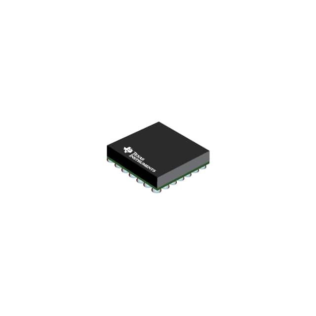
- Part No.:
- SCAN921226HSM
- Manufacturer:
- Texas Instruments
- Category:
- Serializers, Deserializers
- Package:
- 49-LFBGA
- Datasheet:
-
 SCAN921226HSM.pdf
- Description:
- SCAN921226H HIGH TEMPERATURE 20M
- Quantity:
- Payment:

- Shipping:

Inventory:832
Please send an inquiry. Send us your inquiry, and we will respond immediately.
Product details
Overview
SCAN921226HSM from Texas Instruments (formerly National Semiconductor) is a 10-bit Bus LVDS deserializer IC that recovers parallel clock and reconstructs a 10-bit LVCMOS/LVTTL data bus from a single high-speed differential serial stream. It operates at 20–80 MHz input clock rates, delivers 800 Mbps payload data rate, supports IEEE 1149.1 JTAG boundary scan, and features at-speed BIST for interconnect validation in automotive and aerospace backplane systems.
For engineers reviewing the SCAN921226HSM datasheet, SCAN921226HSM pinout, SCAN921226HSM application, or SCAN921226HSM equivalent, this page provides verified functional identity, confirmed 49-ball BGA package mapping, validated 20–80 MHz PLL lock range, real-world lock time metrics (0.29–2.5 µs), and two documented alternative deserializers with explicit interface and timing differences.
Technical Context
The SCAN921226HSM implements a PLL-based clock recovery architecture that locks to embedded clock bits within a 12-bit serial frame (10 data + start/stop), enabling deterministic synchronization without external clock distribution. Its dual-mode operation-synchronization-to-SYNC-patterns (≤2.5 µs lock at 80 MHz) and random-data lock (mean 3.0 µs)-supports both deterministic initialization and hot-insertion into live backplanes.
It integrates IEEE 1149.1 TAP controller with EXTEST and RUNBIST instructions for LVDS interconnect testing at system speed, achieving <10⁻⁷ BER pass criteria. The deserializer outputs ROUT0–ROUT9 and RCLK are CMOS-compatible (15 pF load, 80 MHz max), with LOCK indicating PLL lock status and RCLK_R/F selecting output edge polarity.
Key Specifications
| Parameter | Value and Actual Design Meaning |
|---|---|
| Function | 10-bit Bus LVDS deserializer with embedded clock recovery |
| Input Clock Range | 20–80 MHz REFCLK; enables 800 Mbps payload data rate (10 × fREFCLK) |
| PLL Lock Time | 0.29–0.8 µs (to SYNC patterns), 0.43–18 µs (to random data); critical for deterministic resync |
| Supply Voltage | 3.0–3.6 V; supports industrial temperature range (−40°C to +125°C) |
| Power Consumption | 100–120 mA typical at 80 MHz; <1.0 mA in powerdown mode |
| Interface Standard | IEEE 1149.1 (JTAG) compliant with EXTEST and RUNBIST test modes |
| Package | 49-ball BGA (SLC49a), 7 mm × 7 mm, 0.8 mm pitch |
Pinout & Package
SCAN921226HSM uses a 49-ball BGA package (SLC49a) with 0.8 mm pitch, optimized for high-density backplane and cable interconnect applications. Thermal resistance θJA = 85°C/W; maximum power dissipation = 1.47 W at 25°C.
| Pin/Terminal | Circuit Role | Design Meaning |
|---|---|---|
| RI+, RI− | Bus LVDS differential input | Receives serialized 12-bit stream (10 data + start/stop); threshold ±12 mV differential |
| REFCLK | Reference clock input | Local oscillator reference for PLL; must be stable before power-up for reliable lock |
| ROUT0–ROUT9 | Parallel LVCMOS/LVTTL data outputs | Reconstructed 10-bit bus; drive ≤3 CMOS gates (15 pF) at up to 80 MHz |
| RCLK | Recovered clock output | Phase-aligned to deserialized data; edge polarity controlled by RCLK_R/F |
| LOCK | PLL lock status indicator | Active-low signal; asserts low when PLL locked; used for sync feedback to serializer |
| PWRDN, REN | Power control inputs | Drive both low to enter powerdown; REN low forces ROUT/RCLK into TRI-STATE |
| RCLK_R/F | Output clock edge select | High = rising-edge strobe; low = falling-edge strobe for ROUT data valid window |
| VCC, GND | Power supply terminals | Dual-supply pins (DVCC/AVCC) support noise-isolated analog/digital domains |
Key Features
| Feature | Design Value |
|---|---|
| Random-data lock capability | Enables hot insertion into live backplanes without SYNC pattern dependency; lock time statistically bounded (0.43–18 µs) |
| Embedded clock framing | Start/stop bits guarantee transition every 12-bit cycle, eliminating transmission errors from charged cables |
| At-speed BIST with BER validation | RUNBIST instruction verifies LVDS interconnect integrity at full 800 Mbps; PASS/FAIL reported via RX BIST register |
| Tri-state receiver outputs | REN pin disables ROUT0–ROUT9 and RCLK while preserving LOCK state-critical for multi-drop bus arbitration |
| JTAG boundary scan access | Full IEEE 1149.1 TAP control of digital I/O pins and LVDS interconnect test via EXTEST instruction |
Applications
| Automotive Infotainment Backplane | Aerospace Avionics Data Link |
|---|---|
Use Scenario: Transmitting video/audio control data across vehicle ECU backplanes using unshielded twisted pair (UTP) cabling. IC Role / Device Role / Timing Role: SCAN921226HSM recovers clock and data from serialized BLVDS stream sent by SCAN921025HSM; provides jitter-tolerant 10-bit parallel interface to display controller ASIC. Use Value: Eliminates clock-to-data skew across long traces; 125°C rating ensures reliability in under-hood environments. | Use Scenario: High-integrity sensor data aggregation in flight control systems where hot-swap capability and deterministic lock time are mandatory. IC Role / Device Role / Timing Role: SCAN921226HSM acts as fault-tolerant deserializer in redundant data paths; LOCK signal feeds health monitoring logic for failover decisions. Use Value: Random-lock mode enables insertion during system runtime; RUNBIST validates interconnect integrity before mission-critical data transfer. |
| Industrial PLC I/O Expansion | Military Radar Signal Distribution |
Use Scenario: Extending modular I/O modules over extended backplane distances with minimal connector pin count and EMI resilience. IC Role / Device Role / Timing Role: SCAN921226HSM reconstructs parallel control/status signals from serial BLVDS link; RCLK_R/F allows alignment to legacy controller timing requirements. Use Value: Single differential pair reduces PCB layer count and connector size; 27Ω Bus LVDS drive matches standard backplane impedance. | Use Scenario: Distributing high-speed ADC samples from radar front-end to processing units across ruggedized chassis backplanes. IC Role / Device Role / Timing Role: SCAN921226HSM recovers synchronized 10-bit sample data with sub-microsecond lock assurance; LOCK output triggers sample validity flag. Use Value: Guaranteed transition every 12-bit cycle prevents bit slip during RF-induced transients; −40°C to +125°C operation meets MIL-STD-810G thermal cycling requirements. |
Equivalent & Alternatives
The following parts are listed as comparable options for similar deserializer applications.
| Alternative Part | Technical Difference | Application Difference | Selection Advice |
|---|---|---|---|
| SN65LVDS32 | Single-ended LVDS receiver (no clock recovery); requires separate clock path; no JTAG/BIST | Lacks embedded clock recovery and interconnect test capability; limited to point-to-point links with dedicated clock routing | Select only if system already provides recovered clock and does not require at-speed interconnect validation. |
| DS90CR288A | 28-bit LVDS deserializer with embedded clock; 100–110 MHz range; no JTAG support; different pinout | Higher channel count but incompatible interface protocol; lacks IEEE 1149.1 test access and random-lock capability | Choose for higher bandwidth needs where JTAG testability and hot-insertion are not required. |
Compared with SN65LVDS32 and DS90CR288A, the SCAN921226HSM uniquely combines embedded clock recovery, IEEE 1149.1 testability, and sub-microsecond random-lock timing-making it the only option qualified for safety-critical, hot-pluggable backplane architectures requiring deterministic validation.
Availability
SCAN921226HSM is available at Aetrix Electronics and suitable for automotive infotainment backplanes, aerospace avionics data links, and industrial PLC I/O expansion requiring stable component supply across extended temperature ranges and long production lifecycles.
Supply support for SCAN921226HSM includes scheduled delivery planning, volume procurement assistance, BOM continuity management, traceable sourcing, and lifecycle availability coordination for OEM customers, industrial embedded developers, connected-device designers, and electronics production programs.
Manufacturer
Texas Instruments acquired National Semiconductor in 2011 and maintains full technical and manufacturing continuity for legacy high-reliability interface products.
The SCAN921226HSM belongs to TI's Bus LVDS SerDes chipset family, designed specifically for high-temperature, high-integrity serial backplane communication in safety-critical systems where skew elimination, interconnect testability, and hot-insertion are mandatory.
FAQ
What is the minimum and maximum REFCLK frequency supported by SCAN921226HSM?
The SCAN921226HSM supports REFCLK frequencies from 20 MHz to 80 MHz, corresponding to serial data rates of 240 Mbps to 960 Mbps (12 × fREFCLK). At 80 MHz, the payload data rate is 800 Mbps (10 × fREFCLK). Operation outside this range is not guaranteed per datasheet specifications, and PLL lock cannot be assured below 20 MHz or above 80 MHz.
Does SCAN921226HSM require an external clock source for operation?
Yes, SCAN921226HSM requires a stable external REFCLK signal applied to its REFCLK pin. This reference clock drives the internal PLL for clock recovery and must be active before power-up to ensure deterministic lock behavior. Unlike self-clocked receivers, SCAN921226HSM does not extract timing solely from the incoming BLVDS stream-it uses REFCLK as the local oscillator reference for phase alignment.
How does the LOCK pin function in SCAN921226HSM, and what design actions should follow a LOCK deassertion?
The LOCK pin on SCAN921226HSM is an active-low open-drain output indicating PLL lock status. When LOCK goes high, the deserializer has lost synchronization-causing ROUT0–ROUT9 and RCLK to become invalid. Designers must monitor LOCK and trigger resynchronization, typically by pulsing SYNC1/SYNC2 on the companion SCAN921025HSM serializer. Up to three prior data cycles may contain bit errors after LOCK loss, so application-level error handling is required.
Can SCAN921226HSM operate without sending SYNC patterns from the serializer?
Yes, SCAN921226HSM supports random-data lock mode, allowing it to acquire lock to arbitrary data streams without SYNC pattern transmission. This enables true hot-insertion into live backplanes. However, lock time varies statistically (0.43–18 µs) depending on data pattern characteristics, unlike deterministic SYNC-based lock (≤0.8 µs at 80 MHz). False-lock detection circuitry prevents misalignment to repetitive multi-transition (RMT) patterns.
What is the purpose of the RCLK_R/F pin on SCAN921226HSM, and how does it affect timing?
The RCLK_R/F pin selects the edge polarity of the RCLK output: high configures rising-edge strobing of ROUT0–ROUT9 data, low configures falling-edge strobing. This directly controls the data valid window relative to RCLK-enabling alignment with downstream ASIC timing requirements. The setup/hold margins (e.g., tROS = 0.35×tRCP at 80 MHz) are specified relative to the selected edge, making RCLK_R/F essential for meeting timing closure in mixed-edge systems.
SCAN921226HSM Specifications
- Product attributes
- Attribute value
- Manufacturer:
- Texas Instruments
- Series:
- -
- Package/Case:
- 49-LFBGA
- Packaging:
- Bulk
- Product Status:
- Active
- Function:
- Deserializer
- Data Rate:
- 800Mbps
- Input Type:
- LVDS
- Output Type:
- LVCMOS, LVTTL
- Number of Inputs:
- 1
- Number of Outputs:
- 10
- Voltage - Supply:
- 3V ~ 3.6V
- Operating Temperature:
- -40°C ~ 125°C (TA)
- Grade:
- -
- Qualification:
- -
- Mounting Type:
- Surface Mount
- Supplier Device Package:
- 49-NFBGA (7x7)
SCAN921226HSM FAQ
1.How can I place an order for SCAN921226HSM through Aetrix?
Please submit a Request for Quotation (RFQ) for SCAN921226HSM on Aetrix. Our sales agent will provide a competitive quotation and guide you through the order confirmation once you accept the terms.
2.Are the price and stock information for SCAN921226HSM reliable?
The price and inventory of SCAN921226HSM are updated periodically and may fluctuate due to market conditions. Stock and pricing data are typically refreshed every 24 hours. Quotation validity for SCAN921226HSM is usually 5 days.
3.What payment methods are accepted for SCAN921226HSM?
We accept Wire Transfer, PayPal, Credit Card, Western Union, MoneyGram, and Escrow for SCAN921226HSM transactions.
Note: Certain payment methods may incur a processing fee.
4.How is shipping managed for SCAN921226HSM?
SCAN921226HSM orders can be shipped via leading logistics carriers, including DHL, UPS, FedEx, TNT, or Registered Mail.
Once your SCAN921226HSM order is processed, you will receive an email with the shipment details and tracking number.
Note: Tracking information may take up to 24 hours to appear. Express delivery typically takes 3–5 business days.
5.How can I obtain technical support or documentation for SCAN921226HSM?
For technical support, including SCAN921226HSM datasheets, pinout diagrams, or application guidance, please contact our engineering support team. They can provide detailed documentation and assistance for your SCAN921226HSM requirements.
6.How does Aetrix verify that SCAN921226HSM is sourced from the original manufacturer or authorized distributors?
All SCAN921226HSM products on Aetrix are procured from qualified distributors and authorized channels. Our dedicated quality assurance team conducts strict verification, including traceability checks and, if necessary, third-party testing. This ensures that SCAN921226HSM meets industry standards.
7.What is the process for return or replacement of SCAN921226HSM?
All SCAN921226HSM units undergo pre-shipment inspection (PSI). If there is an issue with SCAN921226HSM, returns or replacements are accepted under the following conditions:
1.Quantity discrepancies, incorrect items, or visible external defects (such as breakage or corrosion), acknowledged by Aetrix.
2.The issue is reported within 90 days of delivery.
3.The SCAN921226HSM part is unused and in its original packaging.
Return procedure for SCAN921226HSM:
1.Submit a request within 90 days.
2.Obtain a Return Material Authorization (RMA) from Aetrix.
SCAN921226HSM Tags

-
SN65HVS880PWPR
Texas Instruments
-
SN65HVS882PWPR
Texas Instruments

-
FIN3386MTDX
onsemi
-
FIN3385MTDX
onsemi

-
SN65LV1023ARHBR
Texas Instruments

-
SN65LV1023ADBR
Texas Instruments
-
SN65LV1224BDBR
Texas Instruments

-
SN65LVDS93ADGGR
Texas Instruments
-
SN65LVDS93DGGR
Texas Instruments

-
TDES954RGZT
Texas Instruments
-
SN65LV1224BRHBT
Texas Instruments

-
DS90UB914QSQE/NOPB
Texas Instruments
Tech Hub

A practical engineering guide to 3.3V and 5V logic compatibility, input thresholds, resistor dividers, translator ICs, MOSFET level shifting, I2C pull-ups, timing limits and power-sequencing risks.

The 74HC595 uses push-pull logic outputs, while the TPIC6B595 uses 50 V open-drain DMOS sinks for higher-power loads. This guide compares timing, current limits, 3.3 V interfacing, load wiring, thermal…

The 74HC595 converts serial data into eight stable parallel outputs. This guide covers pin functions, shift and storage timing, OE and MR behavior, drive-current limits, cascading, voltage compatibilit…

A technical comparison of level-sensitive latches and edge-triggered flip-flops, covering timing windows, setup and hold limits, master–slave operation, time borrowing, race-through, HDL inference and…

A D latch stores one bit while Enable controls when data can pass. This reference covers gate-level operation, truth tables, transparency, setup and hold timing, LE versus OE, common ICs and practical …

An SR latch stores one bit through cross-coupled feedback. This engineering reference covers NOR and NAND implementations, truth tables, forbidden-state recovery, gated operation, switch debouncing, fa…

Latch circuits retain one bit through feedback. This technical reference covers SR and D latches, truth tables, transparency, timing limits, latch-versus-flip-flop behavior, applications and common log…

An engineering guide to LED driver operation, constant-current and constant-voltage outputs, linear and switching topologies, dimming, IC selection, calculations, replacement compatibility, and fault c…

Operational amplifier guide covering op amp basics, feedback, ideal vs real op amps, common configurations, buffer circuits, offset, bias current, gain-bandwidth, slew rate, rail-to-rail limits and sel…

Jumper cables guide covering safe connection order, red and black clamp placement, final ground connection, cable gauge, length, clamp quality, copper vs CCA cables, jump starter comparison and battery…


