
 My Inquiry
 My Account


Texas Instruments SCAN921226HSM/NOPB
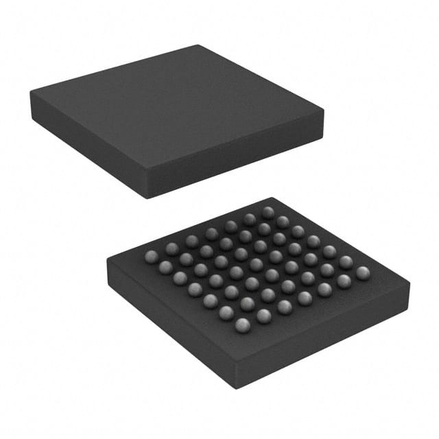
- Part No.:
- SCAN921226HSM/NOPB
- Manufacturer:
- Texas Instruments
- Category:
- Serializers, Deserializers
- Package:
- 49-LFBGA
- Datasheet:
-
 SCAN921226HSM/NOPB.pdf
- Description:
- IC SER/DESER HI TEMP 80MHZ LVDS
- Quantity:
- Payment:

- Shipping:

Inventory:2,974
Please send an inquiry. Send us your inquiry, and we will respond immediately.
Product details
Overview
SCAN921226HSM/NOPB from Texas Instruments is a 10-bit Bus LVDS deserializer IC that recovers parallel data and clock from a single differential serial stream, supporting 20–80 MHz input clock rates (800 Mbps payload), IEEE 1149.1 JTAG compliance, at-speed BIST, and operation up to +125°C. It serves as the receiver in high-reliability backplane or UTP cable interconnects for automotive and aerospace systems.
For engineers reviewing the SCAN921226HSM/NOPB datasheet, SCAN921226HSM/NOPB pinout, SCAN921226HSM/NOPB application, or SCAN921226HSM/NOPB equivalent, key selection criteria include embedded clock recovery performance, random-data lock time (<3.0 μs mean at 80 MHz), JTAG test access, tri-state control via REN, and compatibility with SCAN921025H serializer in chipset deployments.
Technical Context
The SCAN921226HSM/NOPB implements PLL-based clock recovery from a Bus LVDS serial stream containing 10 data bits + 2 embedded clock bits per 12-bit frame. It supports both synchronization-pattern–assisted lock (tDSR2 = 0.29–0.8 μs at 80 MHz) and random-data lock without SYNC patterns.
Its functional states include Data Transfer (LOCK low, ROUT0–ROUT9 valid), Resynchronization (LOCK high → low on relock), Powerdown (PWRDN/REN low, ICCR < 1.0 mA), and Tri-state (REN low, outputs high-impedance). JTAG TAP control enables boundary scan and RUNBIST interconnect testing at system speed.
Key Specifications
| Parameter | Value and Actual Design Meaning |
|---|---|
| Function | 10-bit Bus LVDS deserializer with embedded clock recovery and JTAG test interface |
| Data Rate | 800 Mbps payload (10-bit × 80 MHz TCLK); 960 Mbps serial (12-bit × 80 MHz) |
| Input Clock Range | 20–80 MHz REFCLK; supports synchronization to random data or SYNC patterns |
| Lock Time (Random) | Mean 3.0 μs at 80 MHz (PRBS2¹⁵); enables hot-insertion into live backplanes |
| Supply & Temp | 3.0–3.6 V VCC; operates from −40°C to +125°C ambient |
| Power (Typ) | 105 mA @ 80 MHz (ICCR), <1.0 mA in Powerdown mode |
| JTAG Compliance | Fully IEEE 1149.1–compliant with EXTEST and RUNBIST instructions for LVDS interconnect validation |
Pinout & Package
SCAN921226HSM/NOPB uses a 49-lead NFBGA package (7 mm × 7 mm, 0.8 mm pitch) with exposed thermal pad. Pin functions are validated per TI SNLS185C datasheet Figures 19–20 and Table 2.
| Pin/Terminal | Circuit Role | Design Meaning |
|---|---|---|
| RI+, RI− | Bus LVDS differential input | Receives serialized 12-bit stream (10 data + 2 clock bits); rated for 27 Ω load |
| REFCLK | Reference clock input | Local oscillator reference for PLL; required for lock acquisition and stable RCLK output |
| REN | Receiver enable | Drives ROUT0–ROUT9 and RCLK into tri-state when low; retains LOCK state |
| RCLK_R/F | Output clock edge select | Configures rising/falling edge sampling of ROUT data relative to RCLK |
| LOCK | PLL lock status indicator | Active-low open-drain output; low = valid data; high = loss of lock or initialization |
| ROUT0–ROUT9 | Parallel LVCMOS/LVTTL data outputs | 10-bit recovered parallel bus; drives ≤3 CMOS loads (15 pF) at 80 MHz |
| PWRDN | Global power-down control | Disables PLL and places all outputs in tri-state; reduces ICCR to sub-mA level |
| TCK, TMS, TDI, TDO, TRST | JTAG test access port | Enables boundary scan, EXTEST (LVDS go/no-go), and RUNBIST (at-speed BER <10⁻⁷) |
Key Features
| Feature | Design Value |
|---|---|
| Embedded clock recovery | Eliminates separate clock routing; ensures transition every 12-bit cycle to prevent charged-cable errors |
| At-speed BIST (RUNBIST) | Validates LVDS interconnect integrity at full 800 Mbps; completes in ~28 ms with BER <10⁻⁷ pass threshold |
| Random-data lock capability | Supports hot insertion and open-loop operation without SYNC pattern dependency; mean lock time 3.0 μs at 80 MHz |
| High-temp reliability | Rated for continuous operation at +125°C ambient; qualified per automotive/military thermal stress profiles |
| Single-differential-pair interface | Reduces PCB trace count, connector size, and multi-channel skew vs. parallel buses; simplifies backplane layout |
Applications
| Automotive ADAS Backplane | Industrial PLC I/O Module |
|---|---|
Use Scenario: Transmitting sensor fusion data (camera, radar, IMU) across ruggedized vehicle backplanes with EMI resilience and thermal stability. IC Role / Device Role / Timing Role: Deserializes high-speed video and timing-critical control signals from remote ECUs using Bus LVDS over twisted-pair cabling. Use Value: Enables deterministic 800 Mbps payload throughput with <3.0 μs lock recovery during hot-swap module replacement, meeting ASIL-B timing constraints. |
Use Scenario: Interfacing distributed I/O modules to central controller over long-distance industrial backplanes subject to voltage transients and temperature cycling. IC Role / Device Role / Timing Role: Recovers synchronized 10-bit digital I/O states and timestamped event flags from serialized Bus LVDS links. Use Value: Provides JTAG-accessible diagnostics and at-speed BIST for field-deployed systems, reducing maintenance downtime by validating physical layer integrity pre-boot. |
| Military Avionics Data Link | Aerospace Flight Control Interface |
Use Scenario: Secure, low-SKew transmission of telemetry and command data between avionics LRUs in vibration-prone airframes. IC Role / Device Role / Timing Role: Receives encrypted payload streams from serializer-equipped mission computers; supplies recovered clock and data to FPGA-based processing units. Use Value: Delivers guaranteed transition every 12-bit cycle to prevent bit slips under rapid thermal transients (−40°C to +125°C), satisfying DO-254 Level A requirements. |
Use Scenario: Connecting redundant flight control surface actuators to primary and backup flight computers via fault-tolerant serial interconnects. IC Role / Device Role / Timing Role: Deserializes dual-channel actuator position commands and health-monitoring feedback with LOCK-status monitoring for fail-safe arbitration. Use Value: Supports resynchronization within <0.8 μs using SYNC patterns, enabling sub-millisecond recovery from transient link faults without software intervention. |
Equivalent & Alternatives
The following parts are listed as comparable options for similar Bus LVDS deserializer applications.
| Alternative Part | Technical Difference | Application Difference | Selection Advice |
|---|---|---|---|
| MAX9205EEE+ | 8-bit deserializer; no JTAG; 400 Mbps max; 3.3 V only; no random-lock mode | Limited to lower-bandwidth industrial camera links; lacks IEEE 1149.1 test infrastructure | Select when cost-sensitive, non-military designs require basic deserialization without BIST or high-temp support |
| DS90CR288AMTDX/NOPB | 28-bit LVDS deserializer; no embedded clock recovery; requires separate clock line; no JTAG | Suitable for flat-panel display interfaces where clock/data skew is managed externally | Choose for high-pin-count parallel video paths where separate clock routing is acceptable and test access is handled at system level |
Compared with MAX9205EEE+ and DS90CR288AMTDX/NOPB, SCAN921226HSM/NOPB uniquely integrates JTAG-compliant at-speed BIST, random-data lock capability, and extended temperature operation-making it the only option among the three qualified for safety-critical, high-reliability backplane applications requiring autonomous link validation and thermal robustness.
Availability
SCAN921226HSM/NOPB is available at Aetrix Electronics and suitable for automotive ADAS backplanes, industrial PLC I/O modules, and military avionics data links requiring stable component supply, long-term lifecycle assurance, and traceable sourcing.
Supply support for SCAN921226HSM/NOPB includes scheduled delivery planning, volume procurement assistance, BOM continuity management, traceable sourcing, and lifecycle availability coordination for OEM customers, industrial embedded developers, connected-device designers, and electronics production programs.
Manufacturer
Texas Instruments is a global semiconductor leader specializing in analog, embedded processing, and connectivity technologies with over 50 years of high-reliability component design heritage.
The SCAN921226HSM/NOPB belongs to TI's high-temperature Bus LVDS SerDes chipset family, engineered specifically for deterministic, low-skew, JTAG-testable serial interconnects in harsh-environment automotive, industrial, and aerospace systems.
FAQ
What is the primary function of the SCAN921226HSM/NOPB in a SerDes system?
The SCAN921226HSM/NOPB is a 10-bit Bus LVDS deserializer that recovers parallel data and clock from a single differential serial stream. It works exclusively with the SCAN921025H serializer to form a complete chipset. Its core function is to extract embedded clock information from incoming Bus LVDS data (10 data + 2 clock bits/frame), regenerate a synchronous parallel output bus (ROUT0–ROUT9), and assert LOCK to indicate valid data alignment - all while supporting IEEE 1149.1 JTAG and at-speed BIST.
Does the SCAN921226HSM/NOPB require an external clock source, and if so, what are its requirements?
Yes, the SCAN921226HSM/NOPB requires a stable REFCLK input to operate. REFCLK must be supplied within 20–80 MHz, have a duty cycle of 30–70%, and meet transition time specifications (3–6 ns). This reference clock drives the internal PLL used for clock recovery and determines RCLK output timing. The device cannot achieve lock or produce valid ROUT data without an active REFCLK signal meeting these conditions.
How does the SCAN921226HSM/NOPB handle loss of synchronization during operation?
When the SCAN921226HSM/NOPB loses PLL lock - due to signal interruption, noise, or cable disconnect - the LOCK pin asserts high and ROUT0–ROUT9 enter invalid states. Recovery is initiated by pulsing SYNC1/SYNC2 on the paired SCAN921025H serializer to transmit synchronization patterns. The SCAN921226HSM/NOPB then reacquires lock in ≤0.8 μs (at 80 MHz), after which LOCK goes low and ROUT data resumes validity. No software reset or power cycle is required.
Can the SCAN921226HSM/NOPB operate without the SCAN921025H serializer?
No - the SCAN921226HSM/NOPB is designed exclusively for use with the SCAN921025H serializer as part of a matched chipset. Its Bus LVDS input expects a specific 12-bit framing format (10 data + 2 embedded clock bits), precise jitter tolerance, and timing alignment defined only by the SCAN921025H. While it can lock to random data patterns, interoperability, lock timing guarantees, and BIST functionality depend on the SCAN921025H's compliant output behavior.
What JTAG test capabilities does the SCAN921226HSM/NOPB support, and how are they implemented?
The SCAN921226HSM/NOPB fully implements IEEE 1149.1 JTAG with TCK, TMS, TDI, TDO, and TRST pins. It supports two dedicated test instructions: EXTEST (LVDS-level go/no-go interconnect check) and RUNBIST (at-system-speed interconnect validation with BER <10⁻⁷ pass threshold). RUNBIST executes in ~28 ms at 80 MHz and reports PASS/FAIL via RX BIST data register bits - enabling automated production and field diagnostics without external equipment.
SCAN921226HSM/NOPB Specifications
- Product attributes
- Attribute value
- Manufacturer:
- Texas Instruments
- Series:
- -
- Package/Case:
- 49-LFBGA
- Packaging:
- Tray
- Product Status:
- Active
- Function:
- Deserializer
- Data Rate:
- 800Mbps
- Input Type:
- LVDS
- Output Type:
- LVCMOS, LVTTL
- Number of Inputs:
- 1
- Number of Outputs:
- 10
- Voltage - Supply:
- 3V ~ 3.6V
- Operating Temperature:
- -40°C ~ 125°C (TA)
- Grade:
- -
- Qualification:
- -
- Mounting Type:
- Surface Mount
- Supplier Device Package:
- 49-NFBGA (7x7)
SCAN921226HSM/NOPB FAQ
1.How can I place an order for SCAN921226HSM/NOPB through Aetrix?
Please submit a Request for Quotation (RFQ) for SCAN921226HSM/NOPB on Aetrix. Our sales agent will provide a competitive quotation and guide you through the order confirmation once you accept the terms.
2.Are the price and stock information for SCAN921226HSM/NOPB reliable?
The price and inventory of SCAN921226HSM/NOPB are updated periodically and may fluctuate due to market conditions. Stock and pricing data are typically refreshed every 24 hours. Quotation validity for SCAN921226HSM/NOPB is usually 5 days.
3.What payment methods are accepted for SCAN921226HSM/NOPB?
We accept Wire Transfer, PayPal, Credit Card, Western Union, MoneyGram, and Escrow for SCAN921226HSM/NOPB transactions.
Note: Certain payment methods may incur a processing fee.
4.How is shipping managed for SCAN921226HSM/NOPB?
SCAN921226HSM/NOPB orders can be shipped via leading logistics carriers, including DHL, UPS, FedEx, TNT, or Registered Mail.
Once your SCAN921226HSM/NOPB order is processed, you will receive an email with the shipment details and tracking number.
Note: Tracking information may take up to 24 hours to appear. Express delivery typically takes 3–5 business days.
5.How can I obtain technical support or documentation for SCAN921226HSM/NOPB?
For technical support, including SCAN921226HSM/NOPB datasheets, pinout diagrams, or application guidance, please contact our engineering support team. They can provide detailed documentation and assistance for your SCAN921226HSM/NOPB requirements.
6.How does Aetrix verify that SCAN921226HSM/NOPB is sourced from the original manufacturer or authorized distributors?
All SCAN921226HSM/NOPB products on Aetrix are procured from qualified distributors and authorized channels. Our dedicated quality assurance team conducts strict verification, including traceability checks and, if necessary, third-party testing. This ensures that SCAN921226HSM/NOPB meets industry standards.
7.What is the process for return or replacement of SCAN921226HSM/NOPB?
All SCAN921226HSM/NOPB units undergo pre-shipment inspection (PSI). If there is an issue with SCAN921226HSM/NOPB, returns or replacements are accepted under the following conditions:
1.Quantity discrepancies, incorrect items, or visible external defects (such as breakage or corrosion), acknowledged by Aetrix.
2.The issue is reported within 90 days of delivery.
3.The SCAN921226HSM/NOPB part is unused and in its original packaging.
Return procedure for SCAN921226HSM/NOPB:
1.Submit a request within 90 days.
2.Obtain a Return Material Authorization (RMA) from Aetrix.
SCAN921226HSM/NOPB Tags

-
SN65HVS880PWPR
Texas Instruments
-
SN65HVS882PWPR
Texas Instruments

-
FIN3386MTDX
onsemi
-
FIN3385MTDX
onsemi

-
SN65LV1023ARHBR
Texas Instruments

-
SN65LV1023ADBR
Texas Instruments
-
SN65LV1224BDBR
Texas Instruments

-
SN65LVDS93ADGGR
Texas Instruments
-
SN65LVDS93DGGR
Texas Instruments

-
TDES954RGZT
Texas Instruments
-
SN65LV1224BRHBT
Texas Instruments

-
DS90UB914QSQE/NOPB
Texas Instruments
Tech Hub

A practical engineering guide to 3.3V and 5V logic compatibility, input thresholds, resistor dividers, translator ICs, MOSFET level shifting, I2C pull-ups, timing limits and power-sequencing risks.

The 74HC595 uses push-pull logic outputs, while the TPIC6B595 uses 50 V open-drain DMOS sinks for higher-power loads. This guide compares timing, current limits, 3.3 V interfacing, load wiring, thermal…

The 74HC595 converts serial data into eight stable parallel outputs. This guide covers pin functions, shift and storage timing, OE and MR behavior, drive-current limits, cascading, voltage compatibilit…

A technical comparison of level-sensitive latches and edge-triggered flip-flops, covering timing windows, setup and hold limits, master–slave operation, time borrowing, race-through, HDL inference and…

A D latch stores one bit while Enable controls when data can pass. This reference covers gate-level operation, truth tables, transparency, setup and hold timing, LE versus OE, common ICs and practical …

An SR latch stores one bit through cross-coupled feedback. This engineering reference covers NOR and NAND implementations, truth tables, forbidden-state recovery, gated operation, switch debouncing, fa…

Latch circuits retain one bit through feedback. This technical reference covers SR and D latches, truth tables, transparency, timing limits, latch-versus-flip-flop behavior, applications and common log…

An engineering guide to LED driver operation, constant-current and constant-voltage outputs, linear and switching topologies, dimming, IC selection, calculations, replacement compatibility, and fault c…

Operational amplifier guide covering op amp basics, feedback, ideal vs real op amps, common configurations, buffer circuits, offset, bias current, gain-bandwidth, slew rate, rail-to-rail limits and sel…

Jumper cables guide covering safe connection order, red and black clamp placement, final ground connection, cable gauge, length, clamp quality, copper vs CCA cables, jump starter comparison and battery…


