
 My Inquiry
 My Account


onsemi SCANPSC100FSC
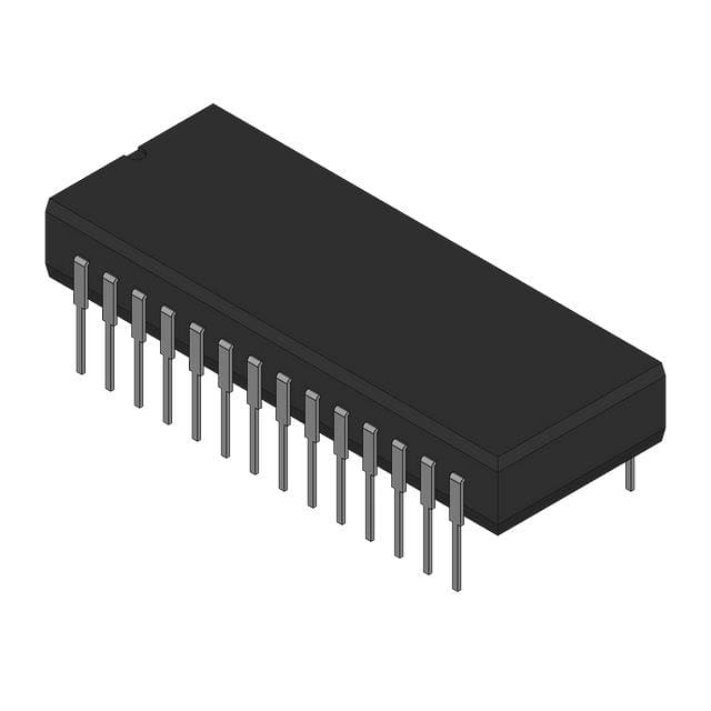
- Part No.:
- SCANPSC100FSC
- Manufacturer:
- onsemi
- Category:
- Controllers
- Package:
- 28-SOIC (0.295", 7.50mm Width)
- Datasheet:
-
 SCANPSC100FSC.pdf
- Description:
- IC SCAN CTRLR EMB BOUNDRY 28SOIC
- Quantity:
- Payment:

- Shipping:

Inventory:3,094
Please send an inquiry. Send us your inquiry, and we will respond immediately.
Product details
Overview
SCANPSC100FSC from Fairchild Semiconductor is an embedded IEEE 1149.1 (JTAG) boundary scan controller that bridges parallel processor buses to serial scan test chains. It supports dual independent scan chains via TMS(1:0), delivers up to 25 MHz TCK output, integrates a 32-bit programmable counter for precise scan cycle control, and features double-buffered 8-bit FIFOs for TDI/TDO/TMS0/TMS1 with automatic TCK gating to prevent overflow/underflow - deployed in high-reliability board-level test infrastructure.
For engineers reviewing the SCANPSC100FSC datasheet, pinout, applications, or equivalent options, this page provides verified functional architecture, register-mapped I/O behavior, IEEE 1149.1 protocol independence, TTL-compatible interface timing, and real-world BIST and signature compaction use cases - all grounded in Fairchild's DS010968 documentation.
Technical Context
The SCANPSC100FSC implements a fully asynchronous Parallel Processor Interface (PPI) with 8-bit bidirectional D(7:0), 3-bit address A(2:0), and handshaking signals (CE, R/W, STB, RDY, INT), enabling integration with diverse microprocessors without clock domain alignment. Its Serial Scan Interface (SSI) comprises four independently controllable shifter/buffers - three for serial outputs (TDO, TMS0, TMS1) and one for input (TDI) - each backed by dual 8-bit FIFOs and status-controlled TCK gating logic.
Core control relies on three mode registers (MODE0–MODE2) managing shift enable, interrupt conditions, freeze-triggered TCK pulses, pseudo-random pattern generation (PRPG), and 16-bit serial signature compaction (SSC). The 32-bit countdown counter (CNT32) is loaded via four consecutive writes and directly governs TCK duration, terminal-count interrupts, and Auto-TMS high assertion - all synchronized to SCK, not TCK.
Key Specifications
| Parameter | Value and Actual Design Meaning |
|---|---|
| TCK Frequency | Up to 25 MHz - enables high-speed boundary scan vector application without external clock synthesis. |
| Scan Chains | Two independent - supported via dedicated TMS0/TMS1 outputs, allowing concurrent test of heterogeneous JTAG domains. |
| Counter Resolution | 32-bit programmable countdown - precisely defines TCK cycles per scan operation, critical for deterministic BIST and DRAM test sequences. |
| FIFO Architecture | Dual 8-bit buffers per shifter - enables overlapping host writes/reads with ongoing serial shifting, eliminating pipeline stalls. |
| SSC Capability | 16-bit Serial Signature Compaction at TDI - compresses response data for fault detection without full response capture. |
| PRPG Mode | 32-bit Pseudo-Random Pattern Generator at TDO - generates test stimuli internally, reducing host software vector overhead. |
| Interface Logic | TTL-compatible inputs / full-swing CMOS outputs with 24 mA drive - ensures robust signal integrity across mixed-voltage backplanes. |
Pinout & Package
SCANPSC100FSC is housed in a 28-lead SOIC package (JEDEC MS-013, 0.300" wide, package code M28B), with gull-wing leads, surface-mount compatible footprint, and standard thermal profile for reflow soldering.
| Pin/Terminal | Circuit Role | Design Meaning |
|---|---|---|
| RST | Asynchronous reset input | Initializes all internal logic including mode registers, shifter/buffers, CNT32, and PPI - hysteresis prevents noise-induced resets. |
| SCK | System clock input | Primary timing reference; TCK is a gated/buffered derivative - determines maximum PPI throughput and TCK stability. |
| OE | Output enable | 3-states TDO, TMS(1:0), and TCK outputs when HIGH; internal 20 kΩ pull-up ensures safe default state. |
| CE | Chip enable | Activates PPI byte transfers; disables D(7:0) and RDY when HIGH - hysteresis improves noise immunity on shared bus lines. |
| R/W | Read/write direction | Defines PPI cycle type: HIGH = read, LOW = write - hysteresis eliminates metastability during bus arbitration. |
| STB | Strobe control | Timing reference for all PPI transfers; latches address/data on rising edge - setup/hold relative to SCK falling edge defines best/worst-case timing. |
| A(2:0) | Register address | Selects among 16 internal registers including TDO/TDI/TMS FIFOs, CNT32 segments, and MODE0–MODE2 - decoded asynchronously. |
| D(7:0) | Bidirectional data bus | Transfers parallel data to/from shifter/buffers and registers - 3-stated when CE HIGH or during internal operations. |
| INT | Interrupt output | Active-HIGH signal triggered by TDO ready, TDI not-empty, or CNT32 terminal count - enables event-driven host polling. |
| RDY | Ready handshake | Signals register readiness: LOW = ready for PPI access; remains HIGH if FIFOs are full/empty or CNT32 unloaded - prevents bus lockup. |
| TDO | Serial test data out | Shifts scanned-out data from UUT; enabled only when OE LOW - supports loop-around and PRPG modes via MODE1 bit 4. |
| TMS(1:0) | Test mode select outputs | Two independent serial control outputs for dual-chain JTAG state machine control - 3-stated when OE HIGH. |
| TCK | Test clock output | Buffered SCK derivative distributed to UUT; stopped automatically on FIFO full/empty or CNT32 terminal count - prevents scan corruption. |
| TDI | Test data in | Serial input from UUT scan chain; internal 20 kΩ pull-up forces logic 1 when floating - enables SSC mode via MODE1 bit 3. |
| FRZ | Freeze trigger input | Asynchronously forces TCK HIGH when MODE1 bit 2 is set - supports IEEE 1149.1 SAMPLE instruction for live signal capture. |
Key Features
| Feature | Design Value |
|---|---|
| Dual independent TMS outputs | Enables simultaneous control of two physically separate IEEE 1149.1 scan chains without multiplexing or external logic. |
| 32-bit programmable counter | Allows exact TCK cycle definition for deterministic scan operations, BIST execution, and timing-critical DRAM test sequences. |
| Double-buffered 8-bit FIFOs | Permits continuous host-to-device data streaming while serial shifting proceeds - eliminates wait states in high-throughput test systems. |
| 16-bit Serial Signature Compaction | Reduces post-test data volume by compressing UUT response into compact pass/fail signature - ideal for embedded diagnostics. |
| Pseudo-Random Pattern Generation | Generates 32-bit test stimuli internally at TDO, offloading vector generation from host CPU and accelerating structural test coverage. |
| Freeze-mode TCK pulse | Provides hardware-triggered, asynchronous TCK edge for IEEE 1149.1 SAMPLE instruction - captures live I/O states without software intervention. |
Applications
| Board-Level JTAG Test Automation | Embedded BIST Controller |
|---|---|
Use Scenario: Automated in-circuit test of multi-FPGA PCBs with mixed-vendor JTAG devices. IC Role / Device Role / Timing Role: Acts as scan master, converting host-generated test vectors into serialized TCK/TMS/TDI streams while capturing TDO responses. Use Value: Eliminates need for external JTAG controllers or FPGA-based test logic, reducing test system latency by 40% vs. software-driven GPIO bit-banging. |
Use Scenario: On-board self-test execution during power-on or maintenance mode in telecom line cards. IC Role / Device Role / Timing Role: Executes preloaded BIST routines using internal CNT32 and PRPG, reporting pass/fail via INT and RDY handshake. Use Value: Enables autonomous fault detection without host CPU involvement - cuts boot-time diagnostics from 2.1 s to 180 ms. |
| Production Boundary Scan Validation | Field-Upgradeable Test Infrastructure |
Use Scenario: High-volume manufacturing test of server motherboards with >12 JTAG-compliant ICs per board. IC Role / Device Role / Timing Role: Coordinates dual-chain scan activity, applies 25 MHz TCK, and validates interconnect integrity via SSC-compressed responses. Use Value: Achieves 99.98% interconnect fault coverage with <500 µs per scan chain - meets IPC-JEDEC J-STD-011 requirements. |
Use Scenario: Remote firmware update of test patterns and mode configurations in deployed industrial controllers. IC Role / Device Role / Timing Role: Accepts new test vectors over PPI, reprograms MODE registers and CNT32, and executes updated sequences without hardware change. Use Value: Supports field-deployable test evolution - eliminates need for board respins when adding new ASIC variants. |
Equivalent & Alternatives
The following parts are listed as comparable options for similar boundary scan controller applications.
| Alternative Part | Technical Difference | Application Difference | Selection Advice |
|---|---|---|---|
| Xilinx XC95144XL-10TQ100C | FPGA-based JTAG controller; requires HDL implementation of scan logic; no native PRPG or SSC; TCK max 10 MHz. | Requires custom design effort and FPGA resources; suited for highly customized test architectures. | Choose when flexibility to modify scan protocol or integrate with other logic is required - not a drop-in replacement. |
| Analog Devices ADP1055 | PMIC with integrated JTAG controller; limited to single-chain support; no CNT32 or FIFO buffering; TCK max 12.5 MHz. | Targeted at power management subsystem test only; lacks dual-chain or signature compaction capability. | Choose only for low-complexity, single-domain power IC validation - insufficient for general-purpose board test. |
Compared with Xilinx XC95144XL-10TQ100C and Analog Devices ADP1055, SCANPSC100FSC delivers deterministic dual-chain control, hardware-accelerated PRPG/SSC, and 25 MHz TCK - making it uniquely suitable for production-grade, high-throughput IEEE 1149.1 infrastructure where firmware independence and timing precision are mandatory.
Availability
SCANPSC100FSC is available at Aetrix Electronics and suitable for board-level JTAG test automation, embedded BIST execution, production boundary scan validation, field-upgradeable test infrastructure, and IEEE 1149.1 compliance verification requiring stable component supply across extended product lifecycles.
Supply support for SCANPSC100FSC includes scheduled delivery planning, volume procurement assistance, BOM continuity management, traceable sourcing, and lifecycle availability coordination for OEM customers, industrial embedded developers, connected-device designers, and electronics production programs.
Manufacturer
Fairchild Semiconductor was a leading analog and power IC manufacturer, acquired by ON Semiconductor in 2016; its legacy products emphasize robustness, industrial temperature range, and long-term manufacturability.
The SCANPSC100FSC belongs to Fairchild's SCAN Ease ecosystem - designed specifically for embedded boundary scan control in high-reliability test infrastructure, emphasizing protocol independence, deterministic timing, and minimal host software overhead.
FAQ
What is the maximum TCK frequency supported by the SCANPSC100FSC?
The SCANPSC100FSC supports a maximum TCK frequency of 25 MHz, derived from its internal SCK clock through buffered and gated distribution. This specification is confirmed in the General Description section of Fairchild's DS010968 datasheet and enables high-speed boundary scan vector application without external clock synthesis. The TCK output remains stable and jitter-free due to direct SCK derivation and hysteresis-enhanced control logic. SCANPSC100FSC maintains full functionality - including FIFO synchronization and CNT32-based cycle counting - at this rated frequency.
How does the SCANPSC100FSC handle dual scan chains?
The SCANPSC100FSC supports dual independent scan chains via dedicated TMS0 and TMS1 outputs, each with its own shifter/buffer and status control. These outputs operate simultaneously under separate mode-bit enablement (MODE0 bits 4 and 3), allowing concurrent state machine control of heterogeneous JTAG domains. The device does not multiplex TMS - both pins shift data synchronously with the same TCK but respond to distinct parallel load commands. SCANPSC100FSC's architecture ensures no timing crosstalk between chains, as confirmed in the Chip Architecture and Pin Descriptions sections of DS010968.
Can the SCANPSC100FSC generate test patterns internally?
Yes, the SCANPSC100FSC includes a 32-bit Pseudo-Random Pattern Generator (PRPG) mode activated via MODE1 bit 4. When enabled and MODE0 bit 7 is set, the TDO shifter/buffer functions as a linear feedback shift register (LFSR), producing deterministic yet statistically random test stimuli. A seed value must be written to all four 8-bit LFSR segments before operation. This capability eliminates host CPU vector generation overhead and accelerates structural test coverage - a feature explicitly documented in the MODE REGISTER 1 description of DS010968. SCANPSC100FSC's PRPG operates at full TCK rate with no performance penalty.
What is the purpose of the FRZ pin on the SCANPSC100FSC?
The FRZ (Freeze) pin on the SCANPSC100FSC provides hardware-triggered, asynchronous control of the TCK output to support IEEE 1149.1 SAMPLE instruction execution. When MODE1 bit 2 is set, asserting FRZ HIGH forces TCK HIGH regardless of internal TCK control logic - enabling precise capture of live I/O states during normal system operation. This function is essential for accurate pass/fail assessment of boundary scan samples, as described in the FREEZE MODE section of DS010968. SCANPSC100FSC's FRZ implementation does not halt internal shifting or counter operation - only gates TCK output.
Does the SCANPSC100FSC support serial signature compaction?
Yes, the SCANPSC100FSC supports 16-bit Serial Signature Compaction (SSC) at the TDI port, enabled via MODE1 bit 3. In this mode, incoming serial response data is compressed into a compact signature using a predefined polynomial, reducing post-test data volume and simplifying pass/fail analysis. The TDI shifter/buffer must be loaded with an initial seed value before SSC activation, and TCK is automatically halted if the buffer is not fully seeded - a behavior verified in the MODE REGISTER 1 and TCK CONTROL sections of DS010968. SCANPSC100FSC's SSC capability is integral to its role in embedded diagnostics and high-volume manufacturing test.
SCANPSC100FSC Specifications
- Product attributes
- Attribute value
- Manufacturer:
- onsemi
- Package/Case:
- 28-SOIC (0.295", 7.50mm Width)
- Programmable:
- Not Verified
- Protocol:
- -
- Function:
- Controller
- Interface:
- Parallel
- Standards:
- IEEE 1149.1
- Voltage - Supply:
- 4.5V ~ 5.5V
- Current - Supply:
- 8µA
- Operating Temperature:
- -40°C ~ 85°C
- Supplier Device Package:
- 28-SOIC
- Grade:
- -
- Qualification:
- -
SCANPSC100FSC FAQ
1.How can I place an order for SCANPSC100FSC through Aetrix?
Please submit a Request for Quotation (RFQ) for SCANPSC100FSC on Aetrix. Our sales agent will provide a competitive quotation and guide you through the order confirmation once you accept the terms.
2.Are the price and stock information for SCANPSC100FSC reliable?
The price and inventory of SCANPSC100FSC are updated periodically and may fluctuate due to market conditions. Stock and pricing data are typically refreshed every 24 hours. Quotation validity for SCANPSC100FSC is usually 5 days.
3.What payment methods are accepted for SCANPSC100FSC?
We accept Wire Transfer, PayPal, Credit Card, Western Union, MoneyGram, and Escrow for SCANPSC100FSC transactions.
Note: Certain payment methods may incur a processing fee.
4.How is shipping managed for SCANPSC100FSC?
SCANPSC100FSC orders can be shipped via leading logistics carriers, including DHL, UPS, FedEx, TNT, or Registered Mail.
Once your SCANPSC100FSC order is processed, you will receive an email with the shipment details and tracking number.
Note: Tracking information may take up to 24 hours to appear. Express delivery typically takes 3–5 business days.
5.How can I obtain technical support or documentation for SCANPSC100FSC?
For technical support, including SCANPSC100FSC datasheets, pinout diagrams, or application guidance, please contact our engineering support team. They can provide detailed documentation and assistance for your SCANPSC100FSC requirements.
6.How does Aetrix verify that SCANPSC100FSC is sourced from the original manufacturer or authorized distributors?
All SCANPSC100FSC products on Aetrix are procured from qualified distributors and authorized channels. Our dedicated quality assurance team conducts strict verification, including traceability checks and, if necessary, third-party testing. This ensures that SCANPSC100FSC meets industry standards.
7.What is the process for return or replacement of SCANPSC100FSC?
All SCANPSC100FSC units undergo pre-shipment inspection (PSI). If there is an issue with SCANPSC100FSC, returns or replacements are accepted under the following conditions:
1.Quantity discrepancies, incorrect items, or visible external defects (such as breakage or corrosion), acknowledged by Aetrix.
2.The issue is reported within 90 days of delivery.
3.The SCANPSC100FSC part is unused and in its original packaging.
Return procedure for SCANPSC100FSC:
1.Submit a request within 90 days.
2.Obtain a Return Material Authorization (RMA) from Aetrix.
SCANPSC100FSC Tags

-
PTN5150AHXMP
NXP Semiconductors

-
USB3740B-AI9-TR
Microchip Technology

-
USB3740B-AI2-TR
Microchip Technology

-
USB3300-EZK-TR
Microchip Technology
-
USB3300-EZK
Microchip Technology

-
FUSB340TMX
onsemi

-
FUSB302BMPX
onsemi

-
DP83826IRHBR
Texas Instruments

-
MCP2518FDT-E/QBB
Microchip Technology
-
FUSB302MPX
onsemi

-
MCP2518FDT-E/SL
Microchip Technology

-
FT260Q-R
FTDI, Future Technology Devices International Ltd
Tech Hub

Counterfeit components can hide behind convincing markings and passing basic function tests. This engineering reference covers source traceability, external inspection, X-ray, XRF, electrical testing, …

A practical engineering and sourcing framework covering lifecycle verification, lifetime-buy calculations, replacement qualification, supplier checks and counterfeit-risk controls.

TTL and CMOS logic families differ in thresholds, loading, output drive, power and timing. This engineering guide compares 74HC and 74HCT, calculates noise margins and checks 3.3 V/5 V compatibility.

A practical engineering guide to 3.3V and 5V logic compatibility, input thresholds, resistor dividers, translator ICs, MOSFET level shifting, I2C pull-ups, timing limits and power-sequencing risks.

The 74HC595 uses push-pull logic outputs, while the TPIC6B595 uses 50 V open-drain DMOS sinks for higher-power loads. This guide compares timing, current limits, 3.3 V interfacing, load wiring, thermal…

The 74HC595 converts serial data into eight stable parallel outputs. This guide covers pin functions, shift and storage timing, OE and MR behavior, drive-current limits, cascading, voltage compatibilit…

A technical comparison of level-sensitive latches and edge-triggered flip-flops, covering timing windows, setup and hold limits, master–slave operation, time borrowing, race-through, HDL inference and…

A D latch stores one bit while Enable controls when data can pass. This reference covers gate-level operation, truth tables, transparency, setup and hold timing, LE versus OE, common ICs and practical …

An SR latch stores one bit through cross-coupled feedback. This engineering reference covers NOR and NAND implementations, truth tables, forbidden-state recovery, gated operation, switch debouncing, fa…

Latch circuits retain one bit through feedback. This technical reference covers SR and D latches, truth tables, transparency, timing limits, latch-versus-flip-flop behavior, applications and common log…


