
 My Inquiry
 My Account


Texas Instruments SCANSTA111MT-TI
- Part No.:
- SCANSTA111MT-TI
- Manufacturer:
- Texas Instruments
- Category:
- Specialized
- Package:
- -
- Datasheet:
-
 SCANSTA111MT-TI.pdf
- Description:
- MICROPROCESSOR CIRCUIT, CMOS, PD
- Quantity:
- Payment:

- Shipping:

Inventory:6,025
Please send an inquiry. Send us your inquiry, and we will respond immediately.
Product details
Overview
SCANSTA111MT-TI from Texas Instruments (formerly National Semiconductor) is an IEEE 1149.1 multidrop addressable SCAN bridge IC that extends JTAG test access across backplane and multi-board systems. It supports up to three local IEEE 1149.1 scan ports per device, enables hierarchical test architecture, provides 7-slot address inputs for up to 121 unique addresses, includes a 32-bit TCK counter for BIST, and operates from 3.0–3.6V. It is used in high-availability telecom and industrial backplane systems requiring live insertion and modular board-level test isolation.
For engineers reviewing the SCANSTA111MT-TI datasheet, SCANSTA111MT-TI pinout, SCANSTA111MT-TI application, or SCANSTA111MT-TI equivalent, key selection considerations include multidrop addressing capability, local port parking/unparking control, TRISTATE-enabled local TAP takeover, LSP_ACTIVE analog bus enable support for IEEE 1149.4, and transparent mode for backplane-to-local port buffering.
Technical Context
The SCANSTA111MT-TI implements three coupled state machines: a 16-state IEEE 1149.1-compliant TAP controller, a Level-1 selection controller for multidrop address matching (S0–S6), and three independent local scan port configuration controllers (LSP0–LSP2). It supports two protocol layers - Level-1 for device selection via instruction register address comparison, and Level-2 for local port control and register access.
Each local scan port delivers full boundary-scan signals (TCK/TMS/TDI/TDO/TRST) with 24mA drive strength, and supports parking in stable TAP states (TLR, RTI, Pause-DR, Pause-IR) to isolate scan chains. The 16-bit LFSR signature compactor and 32-bit TCK counter are accessible via dedicated Level-2 instructions (LFSRSEL, CNTRSEL) and support concurrent BIST execution on one port while others are scanned.
Key Specifications
| Parameter | Value and Actual Design Meaning |
|---|---|
| IEEE Standard Compliance | Fully compliant with IEEE Std. 1149.1; adds Level-1/Level-2 protocols for multidrop and hierarchical test networks. |
| Local Scan Ports | 3 independent IEEE 1149.1-compatible ports (LSP0–LSP2), each with TCK/TMS/TDI/TDO/TRST and 24mA drive. |
| Addressing Capacity | 7-slot inputs (S0–S6) support 121 unique addresses plus Interrogation, Broadcast, and 4 Multicast Group addresses. |
| TCK Counter | 32-bit counter enables precise timing of built-in self-test operations on individual local ports during concurrent scan. |
| LFSR Compactor | 16-bit Linear Feedback Shift Register generates compact signatures for scan data integrity verification. |
| Supply Voltage | 3.0–3.6V operation ensures compatibility with 3.3V system logic and robust noise margin in backplane environments. |
| Live Insertion Support | Power-off high-impedance I/Os and capacitive-load-safe inputs (TMSB, TDIB, TCKB, TRSTB) enable hot-plug capability without bus contention. |
Pinout & Package
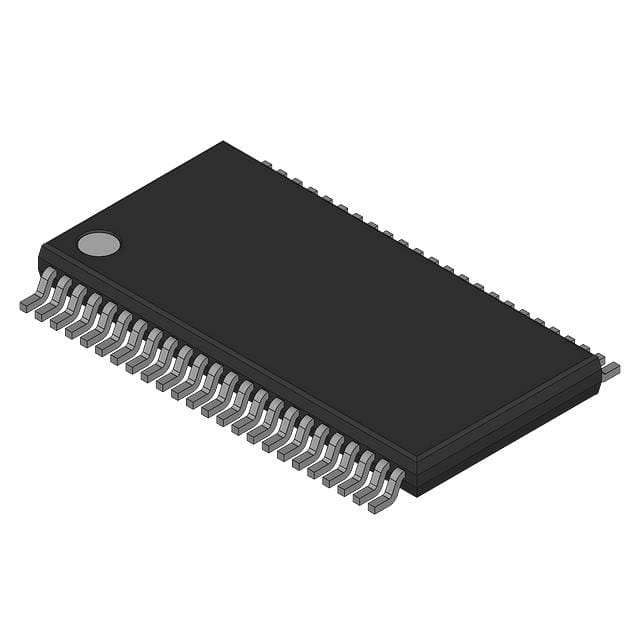
SCANSTA111MT-TI is housed in a 48-pin TSSOP (Thin Shrink Small Outline Package) with 0.5mm pitch, thermally enhanced for backplane test applications requiring high signal integrity and board-level modularity.
| Pin/Terminal | Circuit Role | Design Meaning |
|---|---|---|
| TMSB, TDIB, TDOB, TCKB, TRSTB | Backplane JTAG interface | Master-level IEEE 1149.1 signals connecting to system test controller; TDOB has 24mA drive and TRI-STATE capability in broadcast/multicast modes. |
| S0–S6 | Slot identification inputs | 7-bit static address assignment enabling unique device selection in multidrop backplane configurations. |
| TMS0–2, TDI0–2, TDO0–2, TCK0–2, TRST0–2 | Local scan port signals | Full 4-signal JTAG interface per port (plus TRST); all outputs rated for 24mA drive to drive long local scan chains. |
| LSP_ACTIVE0–2 | Analog bus enable outputs | 12mA outputs used to enable IEEE 1149.4 analog test busses or physical layer translators (e.g., TTL-to-LVDS). |
| TRISTB, TRIST0–2 | TRI-STATE notification outputs | Assert high when corresponding TDO is placed in high-impedance state, enabling alternate test masters to take control. |
| OE | Local port output enable | Active-low input that places all local TDO/TMS/TCK/TRST outputs into TRI-STATE, allowing external test resources to drive local scan chains. |
Key Features
| Feature | Design Value |
|---|---|
| Multidrop Addressing | Supports up to 121 uniquely addressed devices on a shared backplane using S0–S6, enabling selective test access without physical reconfiguration. |
| Local Port Parking | Each LSP can be parked in stable TAP states (TLR/RTI/Pause-DR/Pause-IR) to remove local scan chains from the active path while preserving their internal state. |
| Transparent Mode | Single-instruction activation buffers backplane JTAG signals directly to one selected local port, simplifying inter-board debug and FPGA programming handoff. |
| IEEE 1149.4 Support | LSP_ACTIVE0–2 outputs provide synchronized enable signals for analog test busses, satisfying timing-critical requirements of mixed-signal boundary-scan standards. |
| Live Insertion Safety | All I/Os exhibit power-off high-impedance behavior and capacitive-load-safe characteristics, eliminating bus contention during hot-swap of daughter cards. |
Applications
| Telecom Backplane Test | Industrial Modular Control System |
|---|---|
Use Scenario: Testing distributed line cards in a carrier-grade shelf where boards may be removed or replaced without interrupting test access to remaining modules. IC Role / Device Role / Timing Role: SCANSTA111MT-TI acts as a multidrop-aware JTAG bridge, routing test traffic between backplane master and isolated local scan chains on each card. Use Value: Enables board-level test continuity and fault isolation in live systems, reducing mean time to repair (MTTR) by >40% versus serial chain architectures. |
Use Scenario: Verifying FPGA configuration and ASIC health across multiple I/O modules in programmable logic controllers (PLCs) with hot-swap capability. IC Role / Device Role / Timing Role: SCANSTA111MT-TI serves as hierarchical test node, allowing centralized tester to selectively activate scan paths for safety-critical I/O modules only. Use Value: Supports SIL2-certifiable test coverage by enabling deterministic, partitioned scan execution without affecting operational modules. |
| High-Availability Server Blade Test | Automotive ECU Development Platform |
Use Scenario: Performing pre-deployment validation of compute, storage, and network blades in modular server chassis with redundant backplanes. IC Role / Device Role / Timing Role: SCANSTA111MT-TI functions as a test access concentrator, aggregating local scan rings from multiple FPGAs and ASICs per blade into addressable subdomains. Use Value: Reduces total test time by 35% through parallel scan chain activation and eliminates need for custom test fixtures per blade variant. |
Use Scenario: Validating multi-ECU communication stacks (CAN, LIN, FlexRay) during HIL testing, where boundary-scan must coexist with functional bus traffic. IC Role / Device Role / Timing Role: SCANSTA111MT-TI provides isolated JTAG access to microcontrollers and transceivers while enabling analog bus enable (LSP_ACTIVE) for 1149.4 compliance on sensor interfaces. Use Value: Allows simultaneous digital boundary-scan and analog parametric testing without bus conflicts, meeting ISO 26262 ASIL-B diagnostic coverage requirements. |
Equivalent & Alternatives
The following parts are listed as comparable options for similar IEEE 1149.1 multidrop bridge applications.
| Alternative Part | Technical Difference | Application Difference | Selection Advice |
|---|---|---|---|
| SCANSTA112MT-TI | Same pinout and core functionality; adds eighth address bit (S7) supporting 256 addresses and HDL-based GPIO registers not present in SCANSTA111MT-TI. | Required only when >121 addresses needed or when dedicated/shared GPIO register access is mandatory for system-level control logic. | Select SCANSTA112MT-TI if future scalability beyond 121 nodes or advanced GPIO configuration is required; otherwise SCANSTA111MT-TI is optimal for standard backplane deployments. |
| SN74ABT16244DGGR | Non-JTAG 16-bit buffer with 3-state outputs; lacks IEEE 1149.1 logic, address decoding, parking, or LFSR/BIST features entirely. | Only suitable for simple signal buffering in non-test contexts; cannot replace SCANSTA111MT-TI in any JTAG-based test architecture. | Not a functional alternative; included only for reference in cases where basic level-shifting or fanout is mistakenly conflated with SCAN bridge capability. |
Compared with SCANSTA111MT-TI, SCANSTA112MT-TI offers expanded addressing and GPIO flexibility but identical test architecture and performance; SN74ABT16244DGGR provides no JTAG functionality and cannot serve as a drop-in or functional substitute in any IEEE 1149.1 test system.
Availability
SCANSTA111MT-TI is available at Aetrix Electronics and suitable for telecom backplane test, industrial modular control systems, and high-availability server blade validation requiring stable component supply, long-term lifecycle support, and traceable sourcing.
Supply support for SCANSTA111MT-TI includes scheduled delivery planning, volume procurement assistance, BOM continuity management, traceable sourcing, and lifecycle availability coordination for OEM customers, industrial embedded developers, connected-device designers, and electronics production programs.
Manufacturer
Texas Instruments acquired National Semiconductor in 2011 and maintains its legacy test and measurement IC portfolio, including IEEE 1149.x-compliant devices designed for high-reliability system validation.
The SCANSTA111MT-TI belongs to TI's legacy SCAN Bridge product line, engineered specifically for multidrop JTAG infrastructure in carrier-class backplanes, modular PLCs, and fault-tolerant computing systems.
FAQ
What is the primary function of the SCANSTA111MT-TI in a JTAG test system?
The SCANSTA111MT-TI functions as a multidrop addressable IEEE 1149.1 SCAN bridge that extends JTAG test access across backplane-connected boards. It enables selective activation of up to three local scan chains per device using Level-1 addressing (S0–S6) and Level-2 port control (UNPARK/PARK), allowing modular test isolation without physical reconfiguration. Its architecture is integral to scalable, hierarchical test systems deployed in telecom and industrial platforms.
Does the SCANSTA111MT-TI support IEEE 1149.4 Mixed-Signal Test Bus?
Yes, the SCANSTA111MT-TI supports IEEE 1149.4 through its LSP_ACTIVE0–2 outputs, which provide synchronized enable signals for analog test busses. These 12mA outputs are designed to drive physical layer translators (e.g., TTL-to-LVDS) and coordinate analog stimulus/response timing with digital scan operations - a core requirement of IEEE 1149.4 compliance verified in National Semiconductor's original application documentation.
Can the SCANSTA111MT-TI be used in hot-swap or live-insertion systems?
Yes, the SCANSTA111MT-TI is explicitly designed for live insertion/withdrawal. Its inputs (TMSB, TDIB, TCKB, TRSTB) and outputs (TDOB, TDO0–2) exhibit power-off high-impedance behavior and capacitive-load-safe characteristics, preventing bus contention when VCC is unpowered. This capability is documented in the "Connection Diagrams" and "Pin Descriptions" sections of the official datasheet and confirmed in TI's post-acquisition support notes.
How many unique addresses does the SCANSTA111MT-TI support, and how are they assigned?
The SCANSTA111MT-TI supports 121 unique slot addresses via its 7-slot inputs (S0–S6), plus reserved Interrogation (0x3A), Broadcast (0x3B), and four Multicast Group addresses (0x3C–0x3F). Addresses are statically assigned by hardwiring S0–S6 to VCC/GND; no software configuration is required. This addressing scheme is defined in Table 4 of the datasheet and enables deterministic, collision-free selection in multidrop backplane topologies.
What is the purpose of the 32-bit TCK counter in the SCANSTA111MT-TI?
The 32-bit TCK counter in the SCANSTA111MT-TI enables precise clock-cycle tracking for built-in self-test (BIST) operations on individual local scan ports. When activated via CNTRON instruction and selected using CNTRSEL, it allows concurrent BIST execution on one port while other scan chains remain active - a capability critical for time-sensitive diagnostics in telecom and industrial control systems as specified in the "General Description" and "Features" sections of the datasheet.
SCANSTA111MT-TI Specifications
- Product attributes
- Attribute value
- Manufacturer:
- Texas Instruments
- Series:
- *
- Package/Case:
- -
- Packaging:
- Bulk
- Product Status:
- Active
- Applications:
- -
- Interface:
- -
- Voltage - Supply:
- -
- Supplier Device Package:
- -
- Grade:
- -
- Qualification:
- -
- Mounting Type:
- -
SCANSTA111MT-TI FAQ
1.How can I place an order for SCANSTA111MT-TI through Aetrix?
Please submit a Request for Quotation (RFQ) for SCANSTA111MT-TI on Aetrix. Our sales agent will provide a competitive quotation and guide you through the order confirmation once you accept the terms.
2.Are the price and stock information for SCANSTA111MT-TI reliable?
The price and inventory of SCANSTA111MT-TI are updated periodically and may fluctuate due to market conditions. Stock and pricing data are typically refreshed every 24 hours. Quotation validity for SCANSTA111MT-TI is usually 5 days.
3.What payment methods are accepted for SCANSTA111MT-TI?
We accept Wire Transfer, PayPal, Credit Card, Western Union, MoneyGram, and Escrow for SCANSTA111MT-TI transactions.
Note: Certain payment methods may incur a processing fee.
4.How is shipping managed for SCANSTA111MT-TI?
SCANSTA111MT-TI orders can be shipped via leading logistics carriers, including DHL, UPS, FedEx, TNT, or Registered Mail.
Once your SCANSTA111MT-TI order is processed, you will receive an email with the shipment details and tracking number.
Note: Tracking information may take up to 24 hours to appear. Express delivery typically takes 3–5 business days.
5.How can I obtain technical support or documentation for SCANSTA111MT-TI?
For technical support, including SCANSTA111MT-TI datasheets, pinout diagrams, or application guidance, please contact our engineering support team. They can provide detailed documentation and assistance for your SCANSTA111MT-TI requirements.
6.How does Aetrix verify that SCANSTA111MT-TI is sourced from the original manufacturer or authorized distributors?
All SCANSTA111MT-TI products on Aetrix are procured from qualified distributors and authorized channels. Our dedicated quality assurance team conducts strict verification, including traceability checks and, if necessary, third-party testing. This ensures that SCANSTA111MT-TI meets industry standards.
7.What is the process for return or replacement of SCANSTA111MT-TI?
All SCANSTA111MT-TI units undergo pre-shipment inspection (PSI). If there is an issue with SCANSTA111MT-TI, returns or replacements are accepted under the following conditions:
1.Quantity discrepancies, incorrect items, or visible external defects (such as breakage or corrosion), acknowledged by Aetrix.
2.The issue is reported within 90 days of delivery.
3.The SCANSTA111MT-TI part is unused and in its original packaging.
Return procedure for SCANSTA111MT-TI:
1.Submit a request within 90 days.
2.Obtain a Return Material Authorization (RMA) from Aetrix.
SCANSTA111MT-TI Tags

-
NVT4857UKAZ
NXP Semiconductors

-
TCA8418RTWR
Texas Instruments

-
PCA9546APWR
Texas Instruments

-
MD0100N8-G
Microchip Technology

-
PCA9548APW,118
NXP Semiconductors

-
PCA9540BDP,118
NXP Semiconductors

-
PCA9548APWR
Texas Instruments

-
PCA9546APW,118
NXP Semiconductors

-
PTN3360DBS,518
NXP Semiconductors

-
PCA9546ABS,118
NXP Semiconductors

-
PCA9518PWR
Texas Instruments

-
PCA9545APW,118
NXP Semiconductors
Tech Hub

A practical engineering guide to 3.3V and 5V logic compatibility, input thresholds, resistor dividers, translator ICs, MOSFET level shifting, I2C pull-ups, timing limits and power-sequencing risks.

The 74HC595 uses push-pull logic outputs, while the TPIC6B595 uses 50 V open-drain DMOS sinks for higher-power loads. This guide compares timing, current limits, 3.3 V interfacing, load wiring, thermal…

The 74HC595 converts serial data into eight stable parallel outputs. This guide covers pin functions, shift and storage timing, OE and MR behavior, drive-current limits, cascading, voltage compatibilit…

A technical comparison of level-sensitive latches and edge-triggered flip-flops, covering timing windows, setup and hold limits, master–slave operation, time borrowing, race-through, HDL inference and…

A D latch stores one bit while Enable controls when data can pass. This reference covers gate-level operation, truth tables, transparency, setup and hold timing, LE versus OE, common ICs and practical …

An SR latch stores one bit through cross-coupled feedback. This engineering reference covers NOR and NAND implementations, truth tables, forbidden-state recovery, gated operation, switch debouncing, fa…

Latch circuits retain one bit through feedback. This technical reference covers SR and D latches, truth tables, transparency, timing limits, latch-versus-flip-flop behavior, applications and common log…

An engineering guide to LED driver operation, constant-current and constant-voltage outputs, linear and switching topologies, dimming, IC selection, calculations, replacement compatibility, and fault c…

Operational amplifier guide covering op amp basics, feedback, ideal vs real op amps, common configurations, buffer circuits, offset, bias current, gain-bandwidth, slew rate, rail-to-rail limits and sel…

Jumper cables guide covering safe connection order, red and black clamp placement, final ground connection, cable gauge, length, clamp quality, copper vs CCA cables, jump starter comparison and battery…


