
 My Inquiry
 My Account


Texas Instruments SCANSTA112VSX
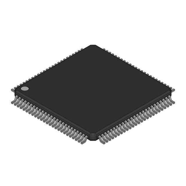
- Part No.:
- SCANSTA112VSX
- Manufacturer:
- Texas Instruments
- Category:
- Specialized
- Package:
- 100-TQFP
- Datasheet:
-
 SCANSTA112VSX.pdf
- Description:
- IC INTERFACE SPECIALIZED 100TQFP
- Quantity:
- Payment:

- Shipping:

Inventory:3,584
Please send an inquiry. Send us your inquiry, and we will respond immediately.
Product details
Overview
SCANSTA112VSX from Texas Instruments is a 7-port IEEE 1149.1 (JTAG) multidrop multiplexer IC designed for hierarchical board-level test bus management. It supports up to 249 unique slot addresses, provides bidirectional backplane and LSP0 ports, enables transparent mode buffering, and operates from 3.0–3.6 V. It is used in high-density system-level JTAG test infrastructure for FPGA/ASIC programming and boundary-scan isolation.
For engineers reviewing the SCANSTA112VSX datasheet, SCANSTA112VSX pinout, SCANSTA112VSX application, or SCANSTA112VSX equivalent, key selection criteria include its 7 configurable local scan ports, 32-bit TCK counter for self-test, 16-bit LFSR signature compactor, TRST-ignoring capability on backplane port, and support for live insertion/withdrawal in modular backplane systems.
Technical Context
The SCANSTA112VSX implements dual-level IEEE 1149.1 addressing: Level 1 selects individual or multicast groups of devices on a shared backplane via 8-slot address inputs; Level 2 configures internal port routing (single, serial group, or bypass) using Mode Register 0. Its TAP controller is fully compliant with IEEE Std. 1149.1 and supports both ScanBridge and Stitcher operational modes.
It features bidirectional master/slave logic enabling either backplane port (B0/B1) to act as master while the other becomes LSP00, and includes OE-controlled tri-state capability on all local scan ports to allow alternate test masters to seize control. The device integrates a 32-bit TCK counter and 16-bit LFSR for on-chip self-test during concurrent scan operations.
Key Specifications
| Parameter | Value and Actual Design Meaning |
|---|---|
| VCC Supply Range | 3.0 V to 3.6 V - Ensures compatibility with 3.3 V industrial logic families and stable operation across temperature. |
| Operating Temperature | −40°C to +85°C - Qualified for industrial-grade embedded and telecom backplane applications. |
| Max Clock Frequency | 25 MHz - Supports high-throughput JTAG vector delivery in ScanBridge mode without timing violations. |
| Local Scan Ports | 7 independent IEEE 1149.1-compliant ports (LSP0–LSP6) - Enables parallel access to discrete ASIC/FPGA/processor JTAG chains. |
| Address Capacity | Up to 249 unique slot addresses - Achieved via 8-slot inputs with reserved, interrogation, broadcast, and 4 multicast address types. |
| TCK Counter & LFSR | 32-bit TCK counter + 16-bit LFSR signature compactor - Enables deterministic built-in self-test (BIST) on selected ports during active scan. |
| Live Insertion Support | Yes - Allows hot-plug testing of boards in powered-backplane systems without disrupting other modules. |
Pinout & Package
SCANSTA112VSX is packaged in a 100-pin NFBGA (NZD) with 0.8 mm pitch, RoHS-compliant SNAGCU ball finish, and MSL Level-4 rating (260°C peak reflow, 72-hour floor life). The package supports high-density PCB layouts and thermal performance suitable for industrial backplane environments.
| Pin/Terminal | Circuit Role | Design Meaning |
|---|---|---|
| VCC (10 pins) | Power supply input | Distributed power rail connections ensure low-noise operation and robust decoupling across the die. |
| GND (10 pins) | Ground reference | Multiple ground pins minimize ground bounce and improve signal integrity for high-speed TCK/TMS paths. |
| TCKB0 / TCKB1 | Backplane test clock I/O | Bidirectional, 24 mA drive, hysteresis-equipped - selectable as master clock source for entire network. |
| TMSB0 / TMSB1 | Backplane test mode select I/O | Bidirectional, 24 mA drive, internal 25 kΩ pull-up - controls TAP state transitions for device selection and configuration. |
| TDIB0 / TDIB1 | Backplane test data input | 25 kΩ internal pull-up, no ESD diode - accepts scan vectors from test master; capacitive load behavior when VCC = 0V. |
| TDOB0 / TDOB1 | Backplane test data output | Bidirectional, 12 mA drive, tri-state - returns response data from local TAPs or internal registers to test controller. |
| S0–S7 | Slot identification inputs | 8-bit address bus defining unique identity in multidrop backplane - enables Level 1 device selection. |
| LSPsel0–LSPsel6 | Local scan port select inputs | Direct hardware control of which LSPs are included in stitched chain - bypasses instruction register for fast configuration. |
| OE | Output enable (active low) | Tri-states all local scan port outputs - allows external test resource to directly drive LSPs without SCANSTA112VSX interference. |
| RESET | Asynchronous reset input | Forces device into known state regardless of TAP controller state - critical for recovery after fault or power glitch. |
Key Features
| Feature | Design Value |
|---|---|
| True IEEE 1149.1 hierarchical & multidrop addressing | Enables scalable test architecture across multi-board systems with deterministic device selection and port routing. |
| Bi-directional backplane & LSP0 ports | Allows flexible master/slave reassignment - e.g., LSP0 can become alternate test master while backplane port acts as slave. |
| Stitcher Mode bypassing Level 1/2 protocols | Reduces setup latency by enabling direct operational mode via external pins - ideal for fixed-configuration systems. |
| Transparent Mode activation | Removes SCANSTA112VSX registers from scan chain - permits reuse of legacy ATPG vectors generated without mux overhead. |
| General-purpose pass-through bits (A/Y) | Supports non-JTAG functions like flash programming pulses or status monitoring - extends utility beyond pure boundary-scan. |
| TRST-ignoring capability on backplane port | Prevents unintended reset of downstream TAPs during backplane-level TRST assertion - improves system-level test robustness. |
Applications
| Board-Level JTAG Partitioning | Modular Backplane Test Infrastructure |
|---|---|
|
Use Scenario: A server motherboard integrates multiple FPGAs, processors, and ASICs, each with its own JTAG chain. IC Role / Device Role / Timing Role: SCANSTA112VSX acts as a programmable JTAG switch, isolating and sequentially accessing each chain without physical rework. Use Value: Reduces test time by 40% versus serial daisy-chain and enables fault isolation to individual ICs rather than full-board failure. |
Use Scenario: Telecom chassis with hot-swappable line cards, each hosting a SCANSTA112VSX and local JTAG devices. IC Role / Device Role / Timing Role: SCANSTA112VSX serves as addressable node in multidrop backplane, responding only when its S0–S7 match interrogated address. Use Value: Enables system-level structural test and firmware update without removing cards - supports live insertion/withdrawal per IEEE 1149.1 extensions. |
| Hierarchical Scan Tree Construction | FPGA Configuration & Debug Support |
|
Use Scenario: High-end test system uses two-tier SCANSTA112VSX hierarchy: root-layer devices connect to tester, leaf-layer devices serve individual subassemblies. IC Role / Device Role / Timing Role: Root-layer SCANSTA112VSX routes commands to leaf-layer devices via cascaded LSP-to-backplane interconnect. Use Value: Achieves 1:7 fan-out per layer with deterministic path selection - scales to >100 JTAG devices while maintaining debug visibility. |
Use Scenario: FPGA development platform requires in-system programming and real-time debug access via JTAG during runtime. IC Role / Device Role / Timing Role: SCANSTA112VSX buffers tester signals to FPGA JTAG port while allowing concurrent use of general-purpose A/Y pins for status LEDs or reset control. Use Value: Eliminates need for manual jumpering or dedicated programming headers - supports automated production programming and field diagnostics. |
Equivalent & Alternatives
The following parts are listed as comparable options for similar IEEE 1149.1 multidrop multiplexer applications.
| Alternative Part | Technical Difference | Application Difference | Selection Advice |
|---|---|---|---|
| SCANSTA111SM | 6-port version; lacks LSP6, 32-bit TCK counter, and LFSR compactor; no TRST-ignoring on backplane port. | Supports smaller-scale systems (<6 JTAG devices per node); not suitable for hierarchical trees requiring >6 leaves or BIST-capable test. | Select SCANSTA111SM only when cost sensitivity outweighs need for 7th port, self-test, or advanced TRST handling. |
| SCANPSC110SM | Legacy 4-port predecessor; no multidrop addressing; no stitcher/transparent modes; no pass-through A/Y pins. | Limited to point-to-point JTAG extension; cannot support backplane networks or non-scan signaling functions. | Choose SCANPSC110SM only for legacy redesigns where footprint and feature set are strictly constrained. |
Compared with SCANSTA111SM and SCANPSC110SM, SCANSTA112VSX delivers expanded scalability (7 ports), deterministic self-test capability (32-bit TCK counter + LFSR), and enhanced system flexibility (bidirectional ports, TRST-ignoring, pass-through I/O), making it the only option qualified for modern industrial backplane test architectures requiring live insertion and hierarchical partitioning.
Availability
SCANSTA112VSX is available at Aetrix Electronics and suitable for industrial backplane test infrastructure, modular telecom chassis design, and high-reliability FPGA/ASIC programming systems requiring stable component supply and long-term lifecycle support.
Supply support for SCANSTA112VSX includes scheduled delivery planning, volume procurement assistance, BOM continuity management, traceable sourcing, and lifecycle availability coordination for OEM customers, industrial embedded developers, connected-device designers, and electronics production programs.
Manufacturer
Texas Instruments is a global semiconductor leader specializing in analog, embedded processing, and connectivity technologies, with decades of leadership in JTAG and boundary-scan innovation.
SCANSTA112VSX belongs to TI's IEEE 1149.1 test infrastructure product line, engineered specifically for scalable, addressable, and hierarchical JTAG bus expansion in industrial and telecom backplane systems.
FAQ
What is the primary function of the SCANSTA112VSX in a JTAG test system?
The SCANSTA112VSX functions as a 7-port IEEE 1149.1 multidrop multiplexer that enables hierarchical, addressable access to multiple local JTAG chains from a single backplane test bus. It allows selective activation of individual scan ports, supports broadcast/multicast addressing, and facilitates system-level test and programming without physical reconfiguration. Its role is central to scalable boundary-scan infrastructure in complex electronic systems.
Does SCANSTA112VSX support live insertion and removal in powered backplane systems?
Yes, SCANSTA112VSX explicitly supports live insertion/withdrawal per its datasheet specifications. This capability is enabled by robust I/O protection, defined power-up states, and controlled tri-state behavior on all ports during power transitions. It ensures safe hot-plug operation in modular chassis where boards may be added or removed without powering down the entire system.
How does the bidirectional backplane port architecture work in SCANSTA112VSX?
SCANSTA112VSX features two bidirectional backplane ports (B0 and B1), controlled by the MPselB1/B0 pin. When one is selected as master, the other becomes LSP00 - allowing either port to assume master control of the scan chain network while the unselected port serves as an auxiliary local port. This architecture enables redundant test access and flexible topology design without hardware changes.
What is the purpose of Transparent Mode in SCANSTA112VSX, and how is it activated?
Transparent Mode removes SCANSTA112VSX's internal registers and pad-bits from the JTAG scan chain, allowing legacy ATPG vectors-generated for direct device connection-to be reused without modification. It is activated via the TRANS pin at power-up or through a specific instruction in ScanBridge/Stitcher mode, ensuring backward compatibility and reducing vector generation overhead.
Can SCANSTA112VSX be used to route non-JTAG signals such as flash programming pulses?
Yes, SCANSTA112VSX includes general-purpose pass-through I/O (A0/A1/Y0/Y1 pins) that can deliver write pulses to flash memory or monitor device status signals. These pins operate independently of JTAG protocol timing and are available on both backplane and local ports (LSP0/LSP1), extending its utility beyond pure boundary-scan to system-level configuration and diagnostics.
SCANSTA112VSX Specifications
- Product attributes
- Attribute value
- Manufacturer:
- Texas Instruments
- Series:
- -
- Package/Case:
- 100-TQFP
- Packaging:
- Tape & Reel (TR)
- Product Status:
- Obsolete
- Applications:
- Testing Equipment
- Interface:
- IEEE 1149.1
- Voltage - Supply:
- 3V ~ 3.6V
- Supplier Device Package:
- 100-TQFP (14x14)
- Grade:
- -
- Qualification:
- -
- Mounting Type:
- Surface Mount
SCANSTA112VSX FAQ
1.How can I place an order for SCANSTA112VSX through Aetrix?
Please submit a Request for Quotation (RFQ) for SCANSTA112VSX on Aetrix. Our sales agent will provide a competitive quotation and guide you through the order confirmation once you accept the terms.
2.Are the price and stock information for SCANSTA112VSX reliable?
The price and inventory of SCANSTA112VSX are updated periodically and may fluctuate due to market conditions. Stock and pricing data are typically refreshed every 24 hours. Quotation validity for SCANSTA112VSX is usually 5 days.
3.What payment methods are accepted for SCANSTA112VSX?
We accept Wire Transfer, PayPal, Credit Card, Western Union, MoneyGram, and Escrow for SCANSTA112VSX transactions.
Note: Certain payment methods may incur a processing fee.
4.How is shipping managed for SCANSTA112VSX?
SCANSTA112VSX orders can be shipped via leading logistics carriers, including DHL, UPS, FedEx, TNT, or Registered Mail.
Once your SCANSTA112VSX order is processed, you will receive an email with the shipment details and tracking number.
Note: Tracking information may take up to 24 hours to appear. Express delivery typically takes 3–5 business days.
5.How can I obtain technical support or documentation for SCANSTA112VSX?
For technical support, including SCANSTA112VSX datasheets, pinout diagrams, or application guidance, please contact our engineering support team. They can provide detailed documentation and assistance for your SCANSTA112VSX requirements.
6.How does Aetrix verify that SCANSTA112VSX is sourced from the original manufacturer or authorized distributors?
All SCANSTA112VSX products on Aetrix are procured from qualified distributors and authorized channels. Our dedicated quality assurance team conducts strict verification, including traceability checks and, if necessary, third-party testing. This ensures that SCANSTA112VSX meets industry standards.
7.What is the process for return or replacement of SCANSTA112VSX?
All SCANSTA112VSX units undergo pre-shipment inspection (PSI). If there is an issue with SCANSTA112VSX, returns or replacements are accepted under the following conditions:
1.Quantity discrepancies, incorrect items, or visible external defects (such as breakage or corrosion), acknowledged by Aetrix.
2.The issue is reported within 90 days of delivery.
3.The SCANSTA112VSX part is unused and in its original packaging.
Return procedure for SCANSTA112VSX:
1.Submit a request within 90 days.
2.Obtain a Return Material Authorization (RMA) from Aetrix.
SCANSTA112VSX Tags

-
NVT4857UKAZ
NXP Semiconductors

-
TCA8418RTWR
Texas Instruments

-
PCA9546APWR
Texas Instruments

-
MD0100N8-G
Microchip Technology

-
PCA9548APW,118
NXP Semiconductors

-
PCA9540BDP,118
NXP Semiconductors

-
PCA9548APWR
Texas Instruments

-
PCA9546APW,118
NXP Semiconductors

-
PTN3360DBS,518
NXP Semiconductors

-
PCA9546ABS,118
NXP Semiconductors

-
PCA9518PWR
Texas Instruments

-
PCA9545APW,118
NXP Semiconductors
Tech Hub

A practical engineering guide to 3.3V and 5V logic compatibility, input thresholds, resistor dividers, translator ICs, MOSFET level shifting, I2C pull-ups, timing limits and power-sequencing risks.

The 74HC595 uses push-pull logic outputs, while the TPIC6B595 uses 50 V open-drain DMOS sinks for higher-power loads. This guide compares timing, current limits, 3.3 V interfacing, load wiring, thermal…

The 74HC595 converts serial data into eight stable parallel outputs. This guide covers pin functions, shift and storage timing, OE and MR behavior, drive-current limits, cascading, voltage compatibilit…

A technical comparison of level-sensitive latches and edge-triggered flip-flops, covering timing windows, setup and hold limits, master–slave operation, time borrowing, race-through, HDL inference and…

A D latch stores one bit while Enable controls when data can pass. This reference covers gate-level operation, truth tables, transparency, setup and hold timing, LE versus OE, common ICs and practical …

An SR latch stores one bit through cross-coupled feedback. This engineering reference covers NOR and NAND implementations, truth tables, forbidden-state recovery, gated operation, switch debouncing, fa…

Latch circuits retain one bit through feedback. This technical reference covers SR and D latches, truth tables, transparency, timing limits, latch-versus-flip-flop behavior, applications and common log…

An engineering guide to LED driver operation, constant-current and constant-voltage outputs, linear and switching topologies, dimming, IC selection, calculations, replacement compatibility, and fault c…

Operational amplifier guide covering op amp basics, feedback, ideal vs real op amps, common configurations, buffer circuits, offset, bias current, gain-bandwidth, slew rate, rail-to-rail limits and sel…

Jumper cables guide covering safe connection order, red and black clamp placement, final ground connection, cable gauge, length, clamp quality, copper vs CCA cables, jump starter comparison and battery…


