
 My Inquiry
 My Account


NXP Semiconductors SCC2681AE1N28,112
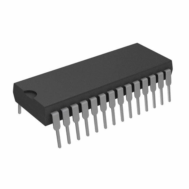
- Part No.:
- SCC2681AE1N28,112
- Manufacturer:
- NXP Semiconductors
- Package:
- 28-DIP (0.600", 15.24mm)
- Datasheet:
-
 SCC2681AE1N28,112.pdf
- Description:
- IC DUART 1MBPS 28DIP
- Quantity:
- Payment:

- Shipping:

Inventory:2,593
Please send an inquiry. Send us your inquiry, and we will respond immediately.
Product details
Overview
SCC2681AE1N28 from NXP Semiconductors (formerly Philips) is an industrial-grade dual universal asynchronous receiver/transmitter (DUART) in a 28-pin DIP package, supporting two independent full-duplex serial channels with quadruple-receiver buffering, programmable 5–8-bit data format, 1–2 stop bits, odd/even/no parity, and up to 115.2 kbaud via internal baud rate generator or external clock. It operates from a single +5 V ±10% supply across –40 °C to +85 °C and integrates a 16-bit counter/timer, 7-bit input port, and 8-bit output port for embedded industrial control and legacy serial interface applications.
For engineers reviewing the SCC2681AE1N28 datasheet, SCC2681AE1N28 pinout, SCC2681AE1N28 application, or SCC2681AE1N28 equivalent, key selection considerations include its 28-pin DIP industrial temperature rating, independent per-channel baud rate selection (including 1×/16× external clock support), false start bit detection, automatic wake-up for multidrop RS-485, and open-drain interrupt outputs configurable as RxRDY/TxRDY signals.
Technical Context
The SCC2681AE1N28 implements two fully independent UART channels sharing a common 8-bit bidirectional data bus (D0–D7), address decoding (A0–A3), and chip enable (CEN) logic. Each channel features separate receiver and transmitter clock selectors, allowing asymmetric operation - e.g., Channel A at 9600 baud (16×) while Channel B runs at 115.2 kbaud (1×) using distinct external clocks on IP3/IP4 and IP5/IP6.
Its timing subsystem integrates an on-chip crystal oscillator (X1/CLK, X2), 18-rate baud generator, and a 16-bit counter/timer usable in timer, counter, or timeout modes. The interrupt system delivers eight maskable conditions through a single active-low open-drain INTRN output, with optional discrete interrupt routing via OP3–OP7 configured as wire-ORable outputs for RxRDY, TxRDY, or C/T events.
Key Specifications
| Parameter | Value and Actual Design Meaning |
|---|---|
| Function | Dual full-duplex asynchronous receiver/transmitter (DUART) with independent channel configuration |
| Supply Voltage | +5 V ±10% - supports industrial rail tolerance without external regulation |
| Operating Temperature | –40 °C to +85 °C - qualified for extended industrial environments |
| Max Data Rate | 115.2 kbaud - achieved via internal baud generator or external 1×/16× clock inputs |
| Receiver Buffering | Quadruple-buffered - reduces CPU interrupt overhead and prevents overrun in burst-mode reception |
| Interrupt Architecture | Single INTRN output with eight maskable sources plus six configurable OP pins for discrete interrupt signaling |
| Package | 28-pin plastic DIP (600 mil) - compatible with through-hole industrial PCB assembly and legacy socketing |
Pinout & Package
SCC2681AE1N28 uses a 28-pin plastic dual in-line package (DIP), 600 mil width, with 0.3 inch row spacing and standard through-hole footprint. Pin 1 is index-corner marked; pins 12 and 23 are not connected (NC).
| Pin/Terminal | Circuit Role | Design Meaning |
|---|---|---|
| 1, 12, 23 | NC | No connection - must remain unconnected per datasheet; no internal tie or function |
| 2–4, 6–7, 16–17, 29–32 | OP0–OP7 | 8-bit programmable output port - individually set/reset; configurable as status/interrupt/DMA/auto-RS485 turn-around signals |
| 5, 8, 40–43 | IP0–IP6 | 7-bit multipurpose input port - includes pull-up (1–4 µA), change-of-state detection on IP0–IP3, and dedicated clock/control roles |
| 9, 10, 25–28, 35–37, 38–39 | WRN, RDN, D0–D7, RXDA, TXDA, X1/CLK, X2, RESET, CEN | Core bus interface - 8-bit data bus with address (A0–A3), strobes (WRN/RDN), chip enable (CEN), reset, and crystal/clock inputs |
| 11, 13–15, 24, 33–34 | RXDB, TXDB, INTRN, OP1, OP3–OP7 | Channel B I/O and interrupt - serial I/O for second UART, active-low interrupt output, and auxiliary output functions |
Key Features
| Feature | Design Value |
|---|---|
| Independent per-channel baud rate selection | Each receiver and transmitter can be assigned different clock sources - internal BRG, 16-bit counter/timer, or external 1×/16× clock - enabling dual-speed multidrop terminal systems |
| Quadruple receiver buffering | Four-level FIFO-like receiver holding registers reduce interrupt frequency by ~75% versus single-buffer UARTs, lowering CPU load in polled or interrupt-driven systems |
| Programmable data framing | 5–8 data bits, 1/1.5/2 stop bits (in 1/16-bit increments), odd/even/no/force parity - supports legacy protocols including IBM 3270 and DEC VT100 |
| Auto RS-485 turn-around | OP0–OP1 can be configured to drive RTSN signals that auto-deactivate after transmission completion - eliminates external logic for half-duplex bus control |
| False start bit rejection | Detects and discards spurious low pulses shorter than valid start-bit duration - improves noise immunity in electrically noisy industrial environments |
Applications
| Industrial PLC Serial Gateway | Legacy Terminal Server |
|---|---|
Use Scenario: Connecting Modbus RTU field devices to a central controller via isolated RS-485 links. IC Role / Device Role / Timing Role: DUART provides dual-channel serial bridging with auto RS-485 turn-around (OP0/OP1) and hardware flow control (IP0/IP1 as CTSN inputs). Use Value: Eliminates need for external direction-control logic and reduces firmware complexity for half-duplex bus arbitration. | Use Scenario: Aggregating serial console access from multiple legacy ASCII terminals (e.g., VT100, ADM-3A) into a TCP/IP network. IC Role / Device Role / Timing Role: Dual UART handles simultaneous terminal sessions; quadruple buffering absorbs keystroke bursts without loss during network latency. Use Value: Sustains 115.2 kbaud per channel with zero character loss under sustained 300–1200 cps typing load. |
| Multidrop Point-of-Sale System | Embedded Test Equipment Interface |
Use Scenario: Coordinating communication between a master controller and multiple slave peripherals (receipt printer, barcode scanner, cash drawer) over shared RS-232/422 lines. IC Role / Device Role / Timing Role: SCC2681AE1N28 acts as serial concentrator with automatic wake-up mode triggered by break detection on either channel. Use Value: Enables low-power sleep state with sub-100 µs wake latency upon receipt of break signal - extends battery life in portable POS units. | Use Scenario: Providing synchronous debug and calibration interfaces for FPGA-based instrumentation with real-time command/response requirements. IC Role / Device Role / Timing Role: Uses counter/timer (CTUR/CTLR) to generate precise 1 ms trigger pulses on OP2/OP3 while maintaining full-duplex serial telemetry on both channels. Use Value: Integrates timing and comms in one IC - avoids adding discrete timer IC and saves 3+ board layers in space-constrained test head designs. |
Equivalent & Alternatives
The following parts are listed as comparable options for similar dual UART applications.
| Alternative Part | Technical Difference | Application Difference | Selection Advice |
|---|---|---|---|
| SCC2692AC1N28 | Same pinout and register map; adds integrated RS-485 driver/receiver on Channel A; higher ICC (15 mA typical) | Eliminates external transceiver for half-duplex RS-485 but requires +5 V only (no ±12 V); not suitable for pure RS-232 designs | Select when RS-485 physical layer integration is required and board space is constrained. |
| TL16C550CPF | 16-byte FIFO per channel; 1.5 MB/s max throughput; 48-pin TQFP; no integrated crystal oscillator or counter/timer | Higher throughput and deeper buffering for high-speed PC-style serial; lacks multidrop wake-up and auto-turnaround features | Select for PC-compatible UART replacement where FIFO depth and speed outweigh industrial temperature and integrated timing needs. |
Compared with SCC2681AE1N28, the SCC2692AC1N28 adds RS-485 PHY integration at the cost of higher power and reduced flexibility for RS-232, while the TL16C550CPF trades industrial robustness and embedded timing features for PC-class throughput and FIFO depth - making SCC2681AE1N28 optimal for deterministic, low-power, multi-protocol industrial serial gateways.
Availability
SCC2681AE1N28 is available at Aetrix Electronics and suitable for industrial automation, legacy terminal interfacing, and embedded test equipment requiring stable component supply across extended temperature ranges and long production lifecycles.
Supply support for SCC2681AE1N28 includes scheduled delivery planning, volume procurement assistance, BOM continuity management, traceable sourcing, and lifecycle availability coordination for OEM customers, industrial embedded developers, connected-device designers, and electronics production programs.
Manufacturer
NXP Semiconductors is a global semiconductor company formed from the spin-off of Philips' semiconductor division, specializing in secure connectivity, automotive, industrial, and IoT solutions with strong legacy support for industrial-grade mixed-signal ICs.
The SCC2681AE1N28 belongs to NXP's legacy communications interface product line, designed specifically for robust, long-lifecycle serial communication in industrial control, point-of-sale, and test instrumentation where reliability, temperature resilience, and protocol flexibility outweigh raw speed.
FAQ
What is the maximum operating temperature range supported by the SCC2681AE1N28?
The SCC2681AE1N28 is rated for industrial operation from –40 °C to +85 °C, with supply voltage tolerance of +5 V ±10%. This specification is confirmed in the Ordering Information table and validated in the Absolute Maximum Ratings and DC Electrical Characteristics sections of the official Philips/NXP datasheet dated April 2004. The SCC2681AE1N28 maintains full functional compliance across this entire range without derating.
Does the SCC2681AE1N28 support automatic RS-485 direction control?
Yes, the SCC2681AE1N28 supports automatic RS-485 turn-around via its programmable output port. When OP0 or OP1 is configured as RTSAN/RTSBN, the SCC2681AE1N28 automatically deactivates the output one bit time after transmission completes - eliminating external direction-control logic. This behavior is documented in the PIN DESCRIPTION table under OP0 and OP1 functions and verified in the Output Port section of the datasheet.
Can the SCC2681AE1N28 operate without an external crystal?
Yes, the SCC2681AE1N28 can operate without an external crystal by using an external clock signal applied to the X1/CLK pin. The device accepts a 1.0–4.0 MHz clock directly; X2 may be left unconnected in this configuration. This capability is explicitly stated in the PIN DESCRIPTION for X1/CLK and confirmed in the Clock Timing section (fCLK = 1.0–4.0 MHz) and Block Diagram description of timing circuitry.
How many interrupt sources does the SCC2681AE1N28 provide, and how are they managed?
The SCC2681AE1N28 provides eight maskable interrupt sources routed through a single active-low open-drain INTRN output. These include RxRDY, TxRDY, break detect, C/T overflow, and input port change events. Interrupt masking is controlled via the Interrupt Mask Register (IMR), and status is read from the Interrupt Status Register (ISR). Additionally, OP3–OP7 can be configured as discrete wire-ORable interrupt outputs - a feature confirmed in the FEATURES list and INTERRUPT CONTROL section of the datasheet.
What is the purpose of the quadruple buffering in the SCC2681AE1N28 receivers?
The quadruple buffering in the SCC2681AE1N28 receivers consists of four cascaded receive holding registers per channel, significantly reducing the risk of receiver overrun during high-burst data reception and lowering interrupt service frequency by up to 75% compared to single-buffer UARTs. This architecture is explicitly described in the DESCRIPTION section and enables reliable operation in interrupt-driven systems handling sustained 115.2 kbaud traffic without CPU overload - a key differentiator for industrial real-time applications.
SCC2681AE1N28,112 Specifications
- Product attributes
- Attribute value
- Manufacturer:
- NXP Semiconductors
- Package/Case:
- 28-DIP (0.600", 15.24mm)
- Series:
- -
- Packaging:
- Tube
- Product Status:
- Obsolete
- Features:
- Configurable GPIO, Internal Oscillator, Timer/Counter
- Number of Channels:
- 2, DUART
- FIFO's:
- -
- Protocol:
- -
- Data Rate (Max):
- 1Mbps
- Voltage - Supply:
- 5V
- With Auto Flow Control:
- Yes
- With IrDA Encoder/Decoder:
- -
- With False Start Bit Detection:
- Yes
- With Modem Control:
- -
- Grade:
- -
- Qualification:
- -
- Mounting Type:
- Through Hole
- Supplier Device Package:
- 28-DIP
SCC2681AE1N28,112 FAQ
1.How can I place an order for SCC2681AE1N28,112 through Aetrix?
Please submit a Request for Quotation (RFQ) for SCC2681AE1N28,112 on Aetrix. Our sales agent will provide a competitive quotation and guide you through the order confirmation once you accept the terms.
2.Are the price and stock information for SCC2681AE1N28,112 reliable?
The price and inventory of SCC2681AE1N28,112 are updated periodically and may fluctuate due to market conditions. Stock and pricing data are typically refreshed every 24 hours. Quotation validity for SCC2681AE1N28,112 is usually 5 days.
3.What payment methods are accepted for SCC2681AE1N28,112?
We accept Wire Transfer, PayPal, Credit Card, Western Union, MoneyGram, and Escrow for SCC2681AE1N28,112 transactions.
Note: Certain payment methods may incur a processing fee.
4.How is shipping managed for SCC2681AE1N28,112?
SCC2681AE1N28,112 orders can be shipped via leading logistics carriers, including DHL, UPS, FedEx, TNT, or Registered Mail.
Once your SCC2681AE1N28,112 order is processed, you will receive an email with the shipment details and tracking number.
Note: Tracking information may take up to 24 hours to appear. Express delivery typically takes 3–5 business days.
5.How can I obtain technical support or documentation for SCC2681AE1N28,112?
For technical support, including SCC2681AE1N28,112 datasheets, pinout diagrams, or application guidance, please contact our engineering support team. They can provide detailed documentation and assistance for your SCC2681AE1N28,112 requirements.
6.How does Aetrix verify that SCC2681AE1N28,112 is sourced from the original manufacturer or authorized distributors?
All SCC2681AE1N28,112 products on Aetrix are procured from qualified distributors and authorized channels. Our dedicated quality assurance team conducts strict verification, including traceability checks and, if necessary, third-party testing. This ensures that SCC2681AE1N28,112 meets industry standards.
7.What is the process for return or replacement of SCC2681AE1N28,112?
All SCC2681AE1N28,112 units undergo pre-shipment inspection (PSI). If there is an issue with SCC2681AE1N28,112, returns or replacements are accepted under the following conditions:
1.Quantity discrepancies, incorrect items, or visible external defects (such as breakage or corrosion), acknowledged by Aetrix.
2.The issue is reported within 90 days of delivery.
3.The SCC2681AE1N28,112 part is unused and in its original packaging.
Return procedure for SCC2681AE1N28,112:
1.Submit a request within 90 days.
2.Obtain a Return Material Authorization (RMA) from Aetrix.
SCC2681AE1N28,112 Tags

-
SC16IS741AIPWJ
NXP Semiconductors

-
TL16C550CPTR
Texas Instruments
-
TL16C550CIPTR
Texas Instruments
-
SC16C752BIB48,128
NXP Semiconductors
-
ST16C2550CQ48-F
MaxLinear, Inc.
-
ST16C2550CJ44-F
MaxLinear, Inc.
-
ST16C2552CJ44-F
MaxLinear, Inc.
-
ST16C1550IQ48-F
MaxLinear, Inc.
-
ST16C2550IQ48-F
MaxLinear, Inc.

-
ST16C554DIQ64-F
MaxLinear, Inc.
-
ST16C554DCQ64-F
MaxLinear, Inc.
-
XR17V352IB113-F
MaxLinear, Inc.
Tech Hub

A practical engineering guide to 3.3V and 5V logic compatibility, input thresholds, resistor dividers, translator ICs, MOSFET level shifting, I2C pull-ups, timing limits and power-sequencing risks.

The 74HC595 uses push-pull logic outputs, while the TPIC6B595 uses 50 V open-drain DMOS sinks for higher-power loads. This guide compares timing, current limits, 3.3 V interfacing, load wiring, thermal…

The 74HC595 converts serial data into eight stable parallel outputs. This guide covers pin functions, shift and storage timing, OE and MR behavior, drive-current limits, cascading, voltage compatibilit…

A technical comparison of level-sensitive latches and edge-triggered flip-flops, covering timing windows, setup and hold limits, master–slave operation, time borrowing, race-through, HDL inference and…

A D latch stores one bit while Enable controls when data can pass. This reference covers gate-level operation, truth tables, transparency, setup and hold timing, LE versus OE, common ICs and practical …

An SR latch stores one bit through cross-coupled feedback. This engineering reference covers NOR and NAND implementations, truth tables, forbidden-state recovery, gated operation, switch debouncing, fa…

Latch circuits retain one bit through feedback. This technical reference covers SR and D latches, truth tables, transparency, timing limits, latch-versus-flip-flop behavior, applications and common log…

An engineering guide to LED driver operation, constant-current and constant-voltage outputs, linear and switching topologies, dimming, IC selection, calculations, replacement compatibility, and fault c…

Operational amplifier guide covering op amp basics, feedback, ideal vs real op amps, common configurations, buffer circuits, offset, bias current, gain-bandwidth, slew rate, rail-to-rail limits and sel…

Jumper cables guide covering safe connection order, red and black clamp placement, final ground connection, cable gauge, length, clamp quality, copper vs CCA cables, jump starter comparison and battery…


