
 My Inquiry
 My Account


NXP Semiconductors SCC2691AC1N24,129
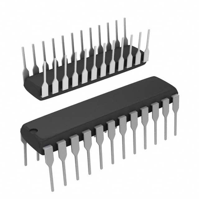
- Part No.:
- SCC2691AC1N24,129
- Manufacturer:
- NXP Semiconductors
- Package:
- 24-DIP (0.300", 7.62mm)
- Datasheet:
-
 SCC2691AC1N24,129.pdf
- Description:
- IC UART 24-DIP
- Quantity:
- Payment:

- Shipping:

Inventory:3,287
Please send an inquiry. Send us your inquiry, and we will respond immediately.
Product details
Overview
SCC2691AC1N24 from NXP Semiconductors (formerly Philips Semiconductors) is a CMOS-LSI universal asynchronous receiver/transmitter (UART) providing full-duplex serial communication with quadruple-buffered receiver, independent receiver/transmitter baud rate selection, and 16-bit programmable counter/timer. It operates from a single +5V supply, supports 5–8 data bits, 1/1.5/2 stop bits, and odd/even/no parity, and is used in industrial terminal systems requiring dual-speed channel operation.
For engineers reviewing the SCC2691AC1N24 datasheet, SCC2691AC1N24 pinout, SCC2691AC1N24 application, or SCC2691AC1N24 equivalent, key selection criteria include TTL-compatible 24-pin DIP packaging, receiver FIFO overrun prevention via RTS handshaking, power-down mode reducing current to 0.5 µA, and support for crystal or external clock inputs up to 4 MHz.
Technical Context
The SCC2691AC1N24 implements a fully integrated UART with independent baud rate generators for receiver and transmitter, selectable from 22 fixed rates (50–115.2 kbaud), non-standard user-defined rates via its 16-bit counter/timer, or external 1X/16X clocks. Its timing architecture includes an on-chip crystal oscillator (3.6864 MHz nominal), clock selectors, and programmable CSR register controlling clock source routing.
It features a 3-level receiver FIFO with RxRDY/FFULL status signaling, automatic RTS assertion when FIFO fills, false start bit detection, line break generation/detection, and multi-mode operation including local/remote loopback and automatic echo. The interrupt system provides a single open-drain INTRN output with seven maskable sources and separate ISR/IMR registers.
Key Specifications
| Parameter | Value and Actual Design Meaning |
|---|---|
| Baud Rates | 22 fixed rates (50–115.2 kbaud); non-standard rates supported via 16-bit counter/timer or external clock - enables dual-speed channel use in clustered terminals. |
| Receiver Buffering | Quadruple-buffered FIFO (3-character depth) - reduces interrupt overhead and prevents overrun in high-throughput interrupt-driven systems. |
| Data Format | 5–8 data bits, 1/1.5/2 stop bits (1/16-bit increments), odd/even/no/force parity - supports legacy and custom serial protocols including RS-232 and proprietary host interfaces. |
| Power Supply | +5 V ±10% - TTL-compatible operation without level-shifting circuitry; eliminates need for auxiliary voltage rails. |
| Operating Temperature | 0°C to +70°C (commercial grade) - validated for stable performance in office automation, point-of-sale, and embedded control environments. |
| Power-Down Current | ≤0.5 µA - oscillator frozen while register contents retained; enables low-energy suspend states in battery-backed or energy-conscious systems. |
| Interrupt Sources | 7 maskable conditions (TxRDY, TxEMT, RxRDY/FFULL, break, C/T terminal count, MPI change) - single INTRN pin simplifies CPU interrupt handling with precise status identification via ISR read. |
Pinout & Package
SCC2691AC1N24 is housed in a 24-pin plastic dual in-line package (DIP), 300 mil width, with 0.3 inch row spacing and through-hole mounting. Pin 1 is located at the left end of the top row (notch side up), and pin numbering proceeds counter-clockwise.
| Pin/Terminal | Circuit Role | Design Meaning |
|---|---|---|
| 1 | RDN | Active-low read strobe - initiates register read cycle when CEN is low; falling edge triggers data placement on D0–D7 bus. |
| 2 | RxD | Receiver serial input - accepts LSB-first asynchronous serial data; sampled on rising edge of internal or external 16X clock. |
| 3 | TxD | Transmitter serial output - drives LSB-first serial stream; held high (marking) when idle or disabled; supports break generation. |
| 4 | MPO | Multi-purpose output - configurable as RTSN, C/TO, TxC1X/TxC16X, RxC1X/RxC16X, TxRDY, or RxRDY/FFULL (open-drain). |
| 5 | MPI | Multi-purpose input - selectable as GPI, CTSN, CTCLK, or RTCLK; internal VCC pull-up (1–4 µA) enables direct connection to open-collector signals. |
| 6–8 | A0–A2 | Address inputs - select one of eight register groups (MR1/MR2, SR/CSR, RHR/THR, etc.) during CPU read/write cycles. |
| 9 | X1/CLK | Clock input - accepts 3.6864 MHz crystal or external clock (0–4 MHz); primary timing reference for BRG, C/T, and internal logic. |
| 10 | X2 | Clock input - crystal termination node; left unconnected or grounded if external clock used instead of crystal. |
| 11 | RESET | Master reset - active-high; clears SR, IMR, ISR, resets mode pointer to MR1, and forces TxD high; required for initialization. |
| 12 | GND | Ground reference - common return for all digital and analog circuitry; must be low-impedance connection to system ground plane. |
| 13 | INTRN | Interrupt request - active-low open-drain output; requires external pull-up; asserts on any enabled interrupt condition per IMR settings. |
| 14 | CEN | Chip enable - active-low; isolates D0–D7 bus in high-impedance state when deasserted; enables parallel interface timing control. |
| 15–22 | D0–D7 | Data bus - bidirectional 8-bit 3-state bus; transfers register contents, commands, and status; direction controlled by WRN/RDN under CEN. |
| 23 | WRN | Active-low write strobe - latches D0–D7 data into selected register on rising edge; synchronized with address A0–A2 and CEN. |
| 24 | VCC | +5 V power supply - supplies entire device; decoupling capacitor (0.1 µF ceramic) recommended adjacent to pin for noise suppression. |
Key Features
| Feature | Design Value |
|---|---|
| Independent Rx/Tx Baud Rate Control | Enables dual-speed channel operation (e.g., host at 9600 baud, peripheral at 115.2 kbaud) without external clock switching logic. |
| 3-Level Receiver FIFO with Handshaking | Automatic RTSN deassertion when FIFO fills prevents data loss in continuous receive streams; eliminates software polling overhead. |
| Programmable 16-Bit Counter/Timer | Generates precise 16X baud clocks for non-standard rates or serves as general-purpose timer/counter with MPO output routing. |
| Multi-Mode Operation | Supports normal full-duplex, automatic echo, local/remote loopback - accelerates firmware validation and hardware bring-up testing. |
| False Start Bit & Line Break Detection | Improves robustness in noisy industrial environments by rejecting spurious transitions and enabling reliable wake-up signaling. |
| Power-Down Mode with Register Retention | Reduces ICCA from 2.5 mA to ≤0.5 µA while preserving configuration - ideal for sleep-wake applications in embedded controllers. |
Applications
| Industrial Terminal Systems | Legacy Equipment Interface |
|---|---|
|
Use Scenario: Clustered intelligent terminals sharing a central controller with asymmetric upstream/downstream data rates. IC Role / Device Role / Timing Role: UART channel controller managing full-duplex serial links between host and multiple remote displays/keypads. Use Value: Independent Rx/Tx baud rate selection allows host to communicate at 115.2 kbaud while terminals respond at 9600 baud - eliminating protocol translation layers. |
Use Scenario: Retrofitting RS-232 connectivity into aging PLCs, CNC machines, or lab instruments lacking native serial ports. IC Role / Device Role / Timing Role: Protocol-transparent bridge converting parallel CPU bus transactions to asynchronous serial framing. Use Value: TTL-compatible I/O and +5 V operation enable direct microcontroller interfacing without level shifters or voltage converters. |
| Embedded Control Panels | Diagnostic Communication Modules |
|
Use Scenario: Operator interface panels in HVAC, building automation, or medical devices requiring local configuration and status reporting. IC Role / Device Role / Timing Role: Serial interface engine supporting command/response protocols over 2-wire or 3-wire RS-232/RS-485 physical layers. Use Value: Quadruple buffering and RxRDY/FFULL interrupts minimize missed keystrokes or status updates during high-priority CPU tasks. |
Use Scenario: Field-service diagnostic tools connecting to automotive ECUs, telecom line cards, or industrial sensors via serial debug ports. IC Role / Device Role / Timing Role: Low-latency serial transceiver supporting break detection, auto-echo, and loopback for protocol validation. Use Value: Built-in line break generation and false start rejection ensure reliable boot-loader synchronization and firmware update handshaking. |
Equivalent & Alternatives
The following parts are listed as comparable options for similar UART applications.
| Alternative Part | Technical Difference | Application Difference | Selection Advice |
|---|---|---|---|
| SCC2692AC1N24 | Pin-compatible 24-pin DIP variant with identical UART core but enhanced counter/timer resolution and extended temperature range (–40°C to +85°C). | Suitable for industrial environments where extended thermal stability and tighter timing control are required. | Select SCC2692AC1N24 when operating outside 0°C–70°C or when sub-microsecond timer accuracy is critical. |
| SC16C2550BIB48 | 32-pin LQFP, 16-byte FIFO, higher max baud (3 Mbps), 3.3 V tolerant I/O - not pin- or register-compatible. | Targets modern 3.3 V systems needing deeper buffering and higher throughput; requires PCB redesign and driver adaptation. | Choose SC16C2550BIB48 only for new designs prioritizing future-proofing, higher speed, and larger buffer depth over drop-in replacement. |
Compared with SCC2691AC1N24, SCC2692AC1N24 offers identical functionality with improved thermal specification and timer precision, while SC16C2550BIB48 delivers greater bandwidth and buffering at the cost of compatibility and voltage-level changes - making SCC2691AC1N24 optimal for cost-sensitive, legacy-anchored commercial deployments.
Availability
SCC2691AC1N24 is available at Aetrix Electronics and suitable for industrial terminal systems, legacy equipment interface modules, embedded control panels, and diagnostic communication modules requiring stable component supply across long production lifecycles.
Supply support for SCC2691AC1N24 includes scheduled delivery planning, volume procurement assistance, BOM continuity management, traceable sourcing, and lifecycle availability coordination for OEM customers, industrial embedded developers, connected-device designers, and electronics production programs.
Manufacturer
NXP Semiconductors is a global semiconductor leader focused on secure connectivity solutions for automotive, industrial, and IoT applications, with roots in Philips' pioneering analog and mixed-signal IC development.
The SCC2691AC1N24 belongs to NXP's legacy communications interface product line, designed specifically for robust, low-power asynchronous serial communication in resource-constrained embedded systems and industrial control equipment.
FAQ
What is the maximum baud rate supported by the SCC2691AC1N24?
The SCC2691AC1N24 supports up to 115.2 kbaud using its internal baud rate generator or external clock inputs. While the datasheet lists 22 fixed rates up to that value, non-standard rates - including those exceeding 115.2 kbaud - are achievable via the programmable 16-bit counter/timer when driven by a crystal or external clock up to 4 MHz. Actual sustained throughput depends on CPU interrupt latency and FIFO management in the host system.
Does the SCC2691AC1N24 require an external crystal, or can it operate with an external clock signal?
The SCC2691AC1N24 can operate with either a 3.6864 MHz crystal connected between X1/CLK and X2 pins, or with an external clock signal applied to X1/CLK (X2 left unconnected or grounded). The device's crystal oscillator circuit is internally configured for fundamental-mode crystals; external clock inputs must meet VIH/VIL thresholds and transition time specs defined in the AC characteristics table. Both options feed the same timing block for baud generation and counter/timer operation.
How does the receiver FIFO and RTS handshaking work together in the SCC2691AC1N24?
In the SCC2691AC1N24, the 3-level receiver FIFO triggers automatic deassertion of the RTSN output (configured via ACR) when the FIFO becomes full. This signals the remote transmitter to pause, preventing overrun. When space becomes available (e.g., after CPU reads RHR), RTSN is reasserted. This hardware flow control operates independently of software polling and requires no CPU intervention - significantly improving reliability in bursty or high-speed receive scenarios.
Can the SCC2691AC1N24 generate a break condition on the TxD line?
Yes, the SCC2691AC1N24 can generate a break condition - a prolonged low state on TxD - by issuing a "start break" command via the Command Register (CR). The break continues until a "stop break" command is issued. During break transmission, the transmitter halts normal character output and holds TxD low; this feature is commonly used for modem control, system reset signaling, or wake-up sequences in multi-processor UART networks.
Is the SCC2691AC1N24 compatible with 3.3 V microcontrollers?
No, the SCC2691AC1N24 is strictly a +5 V TTL-compatible device with VIH minimum of 2.0 V and VIL maximum of 0.8 V - it is not 3.3 V tolerant. Direct interfacing with 3.3 V microcontrollers requires level-shifting circuitry (e.g., TXB0104 or discrete MOSFET translators) on D0–D7, RDN, WRN, CEN, and INTRN lines. Its VCC pin must be supplied with regulated +5 V ±10%, and all timing parameters assume 5 V operation.
SCC2691AC1N24,129 Specifications
- Product attributes
- Attribute value
- Manufacturer:
- NXP Semiconductors
- Package/Case:
- 24-DIP (0.300", 7.62mm)
- Series:
- -
- Packaging:
- Tube
- Product Status:
- Obsolete
- Features:
- Configurable GPIO, Internal Oscillator, Timer/Counter
- Number of Channels:
- 1, UART
- FIFO's:
- -
- Protocol:
- -
- Data Rate (Max):
- -
- Voltage - Supply:
- 5V
- With Auto Flow Control:
- Yes
- With IrDA Encoder/Decoder:
- -
- With False Start Bit Detection:
- Yes
- With Modem Control:
- -
- Grade:
- -
- Qualification:
- -
- Mounting Type:
- Through Hole
- Supplier Device Package:
- 24-DIP
SCC2691AC1N24,129 FAQ
1.How can I place an order for SCC2691AC1N24,129 through Aetrix?
Please submit a Request for Quotation (RFQ) for SCC2691AC1N24,129 on Aetrix. Our sales agent will provide a competitive quotation and guide you through the order confirmation once you accept the terms.
2.Are the price and stock information for SCC2691AC1N24,129 reliable?
The price and inventory of SCC2691AC1N24,129 are updated periodically and may fluctuate due to market conditions. Stock and pricing data are typically refreshed every 24 hours. Quotation validity for SCC2691AC1N24,129 is usually 5 days.
3.What payment methods are accepted for SCC2691AC1N24,129?
We accept Wire Transfer, PayPal, Credit Card, Western Union, MoneyGram, and Escrow for SCC2691AC1N24,129 transactions.
Note: Certain payment methods may incur a processing fee.
4.How is shipping managed for SCC2691AC1N24,129?
SCC2691AC1N24,129 orders can be shipped via leading logistics carriers, including DHL, UPS, FedEx, TNT, or Registered Mail.
Once your SCC2691AC1N24,129 order is processed, you will receive an email with the shipment details and tracking number.
Note: Tracking information may take up to 24 hours to appear. Express delivery typically takes 3–5 business days.
5.How can I obtain technical support or documentation for SCC2691AC1N24,129?
For technical support, including SCC2691AC1N24,129 datasheets, pinout diagrams, or application guidance, please contact our engineering support team. They can provide detailed documentation and assistance for your SCC2691AC1N24,129 requirements.
6.How does Aetrix verify that SCC2691AC1N24,129 is sourced from the original manufacturer or authorized distributors?
All SCC2691AC1N24,129 products on Aetrix are procured from qualified distributors and authorized channels. Our dedicated quality assurance team conducts strict verification, including traceability checks and, if necessary, third-party testing. This ensures that SCC2691AC1N24,129 meets industry standards.
7.What is the process for return or replacement of SCC2691AC1N24,129?
All SCC2691AC1N24,129 units undergo pre-shipment inspection (PSI). If there is an issue with SCC2691AC1N24,129, returns or replacements are accepted under the following conditions:
1.Quantity discrepancies, incorrect items, or visible external defects (such as breakage or corrosion), acknowledged by Aetrix.
2.The issue is reported within 90 days of delivery.
3.The SCC2691AC1N24,129 part is unused and in its original packaging.
Return procedure for SCC2691AC1N24,129:
1.Submit a request within 90 days.
2.Obtain a Return Material Authorization (RMA) from Aetrix.
SCC2691AC1N24,129 Tags

-
SC16IS741AIPWJ
NXP Semiconductors

-
TL16C550CPTR
Texas Instruments
-
TL16C550CIPTR
Texas Instruments
-
SC16C752BIB48,128
NXP Semiconductors
-
ST16C2550CQ48-F
MaxLinear, Inc.
-
ST16C2550CJ44-F
MaxLinear, Inc.
-
ST16C2552CJ44-F
MaxLinear, Inc.
-
ST16C1550IQ48-F
MaxLinear, Inc.
-
ST16C2550IQ48-F
MaxLinear, Inc.

-
ST16C554DIQ64-F
MaxLinear, Inc.
-
ST16C554DCQ64-F
MaxLinear, Inc.
-
XR17V352IB113-F
MaxLinear, Inc.
Tech Hub

A practical engineering guide to 3.3V and 5V logic compatibility, input thresholds, resistor dividers, translator ICs, MOSFET level shifting, I2C pull-ups, timing limits and power-sequencing risks.

The 74HC595 uses push-pull logic outputs, while the TPIC6B595 uses 50 V open-drain DMOS sinks for higher-power loads. This guide compares timing, current limits, 3.3 V interfacing, load wiring, thermal…

The 74HC595 converts serial data into eight stable parallel outputs. This guide covers pin functions, shift and storage timing, OE and MR behavior, drive-current limits, cascading, voltage compatibilit…

A technical comparison of level-sensitive latches and edge-triggered flip-flops, covering timing windows, setup and hold limits, master–slave operation, time borrowing, race-through, HDL inference and…

A D latch stores one bit while Enable controls when data can pass. This reference covers gate-level operation, truth tables, transparency, setup and hold timing, LE versus OE, common ICs and practical …

An SR latch stores one bit through cross-coupled feedback. This engineering reference covers NOR and NAND implementations, truth tables, forbidden-state recovery, gated operation, switch debouncing, fa…

Latch circuits retain one bit through feedback. This technical reference covers SR and D latches, truth tables, transparency, timing limits, latch-versus-flip-flop behavior, applications and common log…

An engineering guide to LED driver operation, constant-current and constant-voltage outputs, linear and switching topologies, dimming, IC selection, calculations, replacement compatibility, and fault c…

Operational amplifier guide covering op amp basics, feedback, ideal vs real op amps, common configurations, buffer circuits, offset, bias current, gain-bandwidth, slew rate, rail-to-rail limits and sel…

Jumper cables guide covering safe connection order, red and black clamp placement, final ground connection, cable gauge, length, clamp quality, copper vs CCA cables, jump starter comparison and battery…


