
 My Inquiry
 My Account


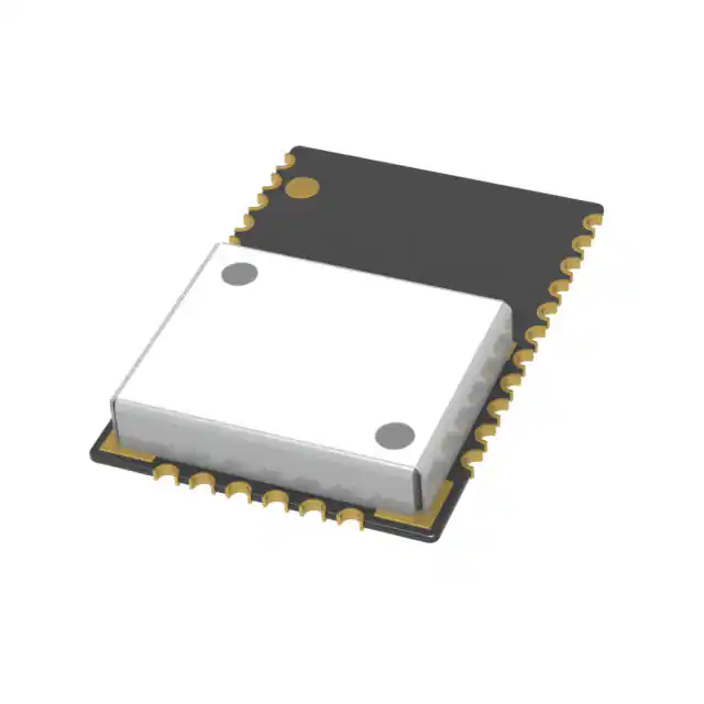
Skyworks Solutions Inc. SE4150L-R
- Part No.:
- SE4150L-R
- Manufacturer:
- Skyworks Solutions Inc.
- Category:
- RF Receivers
- Package:
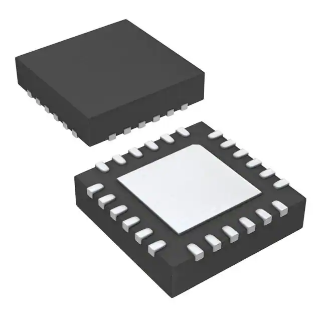
- 24-VFQFN Exposed Pad
- Datasheet:
-
 SE4150L-R.pdf
- Description:
- RF RECEIVER GPS 1575.42MHZ 24QFN
- Quantity:
- Payment:

- Shipping:

Inventory:1,795
Please send an inquiry. Send us your inquiry, and we will respond immediately.
Product details
Overview
SE4150L-R from Skyworks Solutions is a highly integrated L1-band GPS receiver IC with dual RF inputs, on-chip LNA (20 dB gain, 0.9 dB NF), integrated antenna switching, and 2-bit SIGN/MAG digital IF output. It operates from 2.7–3.6 V, draws 15 mA typical active current, and supports 16.368 MHz TCXO reference for GPS navigation in PNDs and mobile handsets.
For engineers reviewing the SE4150L-R datasheet, SE4150L-R pinout, SE4150L-R application, or SE4150L-R equivalent, this page delivers verified technical context, exact pin functions, real-world GPS system integration guidance, hardware configuration modes, and validated alternative options for dual-antenna GNSS front-end design.
Technical Context
The SE4150L-R implements a single-conversion architecture with integrated image-reject low-IF mixer, on-die 3rd-order Butterworth IF filter (centered at 4.092 MHz, 2.2 MHz BW), and linear AGC providing 50 dB gain control range. Its PLL synthesizer includes fully integrated VCO and loop filter, optimized for 16.368 MHz reference input.
It features two independent RF paths-LNA_IN (pin 4) with high-linearity LNA and ANT1_IN (pin 3) for external active antenna-with automatic antenna switching controlled by ANT_DET (pin 8) based on detected bias current (>1 mA). Hardware configuration via HW_0/HW_1 pins selects between Hi/Lo LNA gain (20/17 dB) and Hi/Lo mixer gain (32/24 dB).
Key Specifications
| Parameter | Value and Actual Design Meaning |
|---|---|
| LNA Noise Figure | 0.9 dB typical - enables high-sensitivity GPS reception down to –150 dBm signal levels in obstructed environments. |
| IF Output Format | 2-bit SIGN/MAG digital interface - directly compatible with standard GPS baseband ICs without external ADC. |
| Supply Voltage Range | 2.7 V to 3.6 V - supports single-supply operation with common 3.3 V system rails and low-power battery-powered designs. |
| Active Supply Current | 15 mA typical - balances performance and power efficiency for portable GPS receivers. |
| Standby Current | <10 µA - enables ultra-low-power wake-on-GPS functionality in always-on location-aware devices. |
| IF Center Frequency | 4.092 MHz (with 16.368 MHz ref.) - fixed low-IF architecture simplifies baseband filtering and reduces image interference. |
| Antenna Switch Threshold | 1 mA detection threshold with hysteresis - reliably discriminates active vs. passive antenna presence without false triggering. |
Pinout & Package
SE4150L-R is housed in a 4 × 4 × 0.9 mm, 24-pin QFN package with exposed die pad for thermal management and grounding. The package is Pb-free, RoHS compliant, and halogen free.
| Pin/Terminal | Circuit Role | Design Meaning |
|---|---|---|
| VAGC (1) | AGC filter node | Connects to 10 nF capacitor to GND - sets AGC loop time constant (~10 ms settling); critical for dynamic signal adaptation. |
| ANT_BIAS (2) | Active antenna bias supply | Provides DC bias to external active antenna via coax socket choke - enables antenna current sensing and auto-switching. |
| ANT1_IN (3) | External antenna RF input | DC-biased input for active GNSS antenna - requires DC blocking capacitor; routed to ANT_SW_OUT when ANT_DET = HIGH. |
| LNA_IN (4) | Passive antenna RF input | Direct connection point for passive GNSS antenna element - feeds internal LNA; selected when no external antenna is detected. |
| RX_EN (5) | Global receiver enable | Pull to VDDN to activate full RF chain; internal 200 kΩ pull-down ensures safe default standby state. |
| VCC_LNA (6) | LNA power control | Connect to VCC to enable LNA (adds ~5 mA); tie to GND to disable LNA - enables flexible power/performance trade-offs. |
| ANT_SW_OUT (7) | Switched RF output | Single-ended 50 Ω output feeding mixer - carries either LNA_IN or ANT1_IN path depending on ANT_DET logic state. |
| ANT_DET (8) | Antenna detect I/O | Logic output indicating active antenna presence (HIGH = >1 mA sensed); also accepts override input (<10 kΩ) for host-controlled switching. |
| CLK_OUT (21) | Digital IF sample clock | 16.368 MHz CMOS clock output - drives baseband IC sampling; remains active in standby if CLK_EN = HIGH. |
| SIGN / MAG (20/19) | Digital IF data outputs | 2-bit ADC outputs latched on falling edge of CLK_OUT - require re-sampling on rising edge at baseband for optimal timing margin. |
Key Features
| Feature | Design Value |
|---|---|
| Dual RF input with automatic antenna switching | Enables seamless transition between internal passive and external active antennas without host firmware intervention. |
| Integrated 3rd-order IF filter (2.2 MHz BW, 4.092 MHz CF) | Eliminates need for external SAW or ceramic filters - reduces BOM count and layout sensitivity while maintaining selectivity. |
| Hardware-configurable LNA/mixer linearity | HW_0/HW_1 pins select Hi/Lo gain modes - allows optimization for co-located interference (e.g., cellular bands) or low-noise PND use. |
| On-chip PLL with integrated VCO and loop filter | Removes external loop filter components - simplifies design, improves phase noise stability (–82 dBc/Hz @ 1 kHz offset), and saves board space. |
| Low-noise LNA (0.9 dB NF, 20 dB gain) | Maximizes system sensitivity - contributes dominantly to overall cascaded noise figure of 1.2 dB typical. |
Applications
| Personal Navigation Devices (PNDs) | Smartphone GPS Front-End |
|---|---|
Use Scenario: Portable automotive navigation unit with built-in passive patch antenna and optional external active antenna jack. IC Role / Device Role / Timing Role: GPS RF front-end IC handling L1-band signal acquisition, antenna selection, and digitized IF output to baseband processor. Use Value: Dual-input architecture eliminates manual antenna selection; low 1.2 dB system NF ensures reliable cold-start TTFF indoors and under foliage. |
Use Scenario: Multi-radio smartphone integrating GPS alongside LTE/Wi-Fi/BT, requiring high isolation and minimal PCB area. IC Role / Device Role / Timing Role: Standalone GPS receiver IC providing 2-bit IF output synchronized to 16.368 MHz TCXO clock for precise timing alignment. Use Value: Integrated LNA and IF filter reduce external component count; hardware gain modes allow dynamic adjustment to avoid desensitization from nearby transmitters. |
| Asset Tracking Telematics | Wearable Location Devices |
Use Scenario: Battery-powered vehicle tracker with long-term deployment, requiring ultra-low standby power and robust antenna handling. IC Role / Device Role / Timing Role: GPS signal conditioning and digitization IC enabling periodic wake-up, signal acquisition, and position reporting. Use Value: <10 µA standby current extends battery life; ANT_DET-driven auto-switching maintains GPS lock during antenna cable insertion/removal. |
Use Scenario: Compact wearable fitness tracker needing embedded GNSS for outdoor activity logging with minimal size and power budget. IC Role / Device Role / Timing Role: Miniaturized GPS receiver IC delivering high-sensitivity positioning using compact 4×4 mm QFN footprint. Use Value: 4×4×0.9 mm QFN package fits tight mechanical envelopes; 15 mA active current enables sub-10-second TTFF without overheating. |
Equivalent & Alternatives
The following parts are listed as comparable options for similar GPS receiver IC applications.
| Alternative Part | Technical Difference | Application Difference | Selection Advice |
|---|---|---|---|
| MAX2769CTJ+T | 3.3 V single-supply, 3-bit IF output, no integrated LNA - requires external LNA for comparable sensitivity. | Higher external component count; lacks antenna switching and current detection logic. | Preferred where cost-sensitive designs can accommodate discrete LNA and separate antenna control logic. |
| uBlox UBX-M8030-KT | Integrated GPS/Galileo/GLONASS multi-constellation receiver with embedded processor - not pin-compatible, larger footprint. | Delivers NMEA output and position calculation onboard; eliminates need for external baseband processing. | Chosen when full positioning engine functionality is required rather than raw IF data for custom baseband implementation. |
Compared with MAX2769CTJ+T and uBlox UBX-M8030-KT, the SE4150L-R uniquely combines integrated LNA, dual-antenna switching, and 2-bit IF output in a compact QFN - making it optimal for cost- and size-constrained GPS front-ends requiring host-based baseband processing and automatic antenna management.
Availability
SE4150L-R is available at Aetrix Electronics and suitable for personal navigation devices, telematics asset trackers, and smartphone GPS front-end modules requiring stable component supply, consistent parametric performance, and long-term lifecycle support.
Supply support for SE4150L-R includes scheduled delivery planning, volume procurement assistance, BOM continuity management, traceable sourcing, and lifecycle availability coordination for OEM customers, industrial embedded developers, connected-device designers, and electronics production programs.
Manufacturer
Skyworks Solutions is a global leader in high-performance analog semiconductors, specializing in RF, wireless infrastructure, and precision timing solutions for mobile, automotive, and IoT markets.
The SE4150L-R belongs to Skyworks' GPS receiver IC product line, engineered specifically for low-power, high-sensitivity L1-band GNSS front-end applications in space-constrained portable electronics.
FAQ
What is the primary function of the SE4150L-R in a GPS system?
The SE4150L-R serves as a complete GPS RF front-end IC, performing L1-band signal amplification, frequency conversion, IF filtering, AGC, and 2-bit digitization. It interfaces directly with a baseband processor via SIGN/MAG/CLK_OUT signals and manages dual-antenna selection autonomously - eliminating the need for external LNAs, filters, or switch controllers in the SE4150L-R signal chain.
How does the SE4150L-R handle antenna selection between internal and external sources?
The SE4150L-R uses its integrated antenna current detector to monitor current flow through ANT_BIAS (pin 2). When >1 mA is detected - indicating an active external antenna - ANT_DET (pin 8) asserts HIGH, routing the RF path from ANT1_IN (pin 3) to ANT_SW_OUT (pin 7). If no current is sensed, ANT_DET goes LOW and selects LNA_IN (pin 4) instead. This switching can be overridden by driving ANT_DET externally.
What are the hardware configuration options for LNA and mixer gain on the SE4150L-R?
The SE4150L-R supports four combinations via HW_0 (pin 16) and HW_1 (pin 17): Hi Gain LNA (20 dB, –6 dBm IIP3) + Hi Gain Mixer (32 dB), Lo Gain LNA (17 dB, –12 dBm IIP3) + Lo Gain Mixer (24 dB), or mixed modes. These settings let designers optimize for sensitivity (Hi Gain) or linearity in interference-rich environments (Lo Gain), all without software intervention.
Can the SE4150L-R operate without an external TCXO?
No - the SE4150L-R requires an external 16.368 MHz TCXO connected to TCXO_IN (pin 15) to generate its local oscillator. The device includes VCC_TCXO (pin 13) to power the TCXO, but it does not contain an internal crystal oscillator or frequency synthesis capable of standalone operation. A clipped sine-wave TCXO output is mandatory for proper PLL locking.
What is the significance of the 2-bit SIGN/MAG digital IF output in the SE4150L-R?
The 2-bit SIGN/MAG output provides a simplified, low-pin-count digital interface to GPS baseband processors - replacing traditional analog IF or higher-resolution ADCs. SIGN indicates polarity and MAG indicates magnitude of the IF signal; together they enable efficient correlation and tracking in the baseband. This architecture reduces interface complexity, power, and PCB routing compared to 4+ bit ADCs, while maintaining sufficient dynamic range for GPS acquisition.
SE4150L-R Specifications
- Product attributes
- Attribute value
- Manufacturer:
- Skyworks Solutions Inc.
- Series:
- SiGe
- Package/Case:
- 24-VFQFN Exposed Pad
- Packaging:
- Tape & Reel (TR)
- Product Status:
- Obsolete
- Frequency:
- 1575.42MHz
- Sensitivity:
- -
- Data Rate (Max):
- -
- Modulation or Protocol:
- GPS
- Applications:
- GPS Receiver
- Current - Receiving:
- 15mA
- Data Interface:
- PCB, Surface Mount
- Memory Size:
- -
- Antenna Connector:
- PCB, Surface Mount
- Features:
- -
- Voltage - Supply:
- 2.7V ~ 3.6V
- Operating Temperature:
- -40°C ~ 85°C
- Grade:
- -
- Qualification:
- -
- Mounting Type:
- Surface Mount
- Supplier Device Package:
- 24-QFN (4x4)
SE4150L-R FAQ
1.How can I place an order for SE4150L-R through Aetrix?
Please submit a Request for Quotation (RFQ) for SE4150L-R on Aetrix. Our sales agent will provide a competitive quotation and guide you through the order confirmation once you accept the terms.
2.Are the price and stock information for SE4150L-R reliable?
The price and inventory of SE4150L-R are updated periodically and may fluctuate due to market conditions. Stock and pricing data are typically refreshed every 24 hours. Quotation validity for SE4150L-R is usually 5 days.
3.What payment methods are accepted for SE4150L-R?
We accept Wire Transfer, PayPal, Credit Card, Western Union, MoneyGram, and Escrow for SE4150L-R transactions.
Note: Certain payment methods may incur a processing fee.
4.How is shipping managed for SE4150L-R?
SE4150L-R orders can be shipped via leading logistics carriers, including DHL, UPS, FedEx, TNT, or Registered Mail.
Once your SE4150L-R order is processed, you will receive an email with the shipment details and tracking number.
Note: Tracking information may take up to 24 hours to appear. Express delivery typically takes 3–5 business days.
5.How can I obtain technical support or documentation for SE4150L-R?
For technical support, including SE4150L-R datasheets, pinout diagrams, or application guidance, please contact our engineering support team. They can provide detailed documentation and assistance for your SE4150L-R requirements.
6.How does Aetrix verify that SE4150L-R is sourced from the original manufacturer or authorized distributors?
All SE4150L-R products on Aetrix are procured from qualified distributors and authorized channels. Our dedicated quality assurance team conducts strict verification, including traceability checks and, if necessary, third-party testing. This ensures that SE4150L-R meets industry standards.
7.What is the process for return or replacement of SE4150L-R?
All SE4150L-R units undergo pre-shipment inspection (PSI). If there is an issue with SE4150L-R, returns or replacements are accepted under the following conditions:
1.Quantity discrepancies, incorrect items, or visible external defects (such as breakage or corrosion), acknowledged by Aetrix.
2.The issue is reported within 90 days of delivery.
3.The SE4150L-R part is unused and in its original packaging.
Return procedure for SE4150L-R:
1.Submit a request within 90 days.
2.Obtain a Return Material Authorization (RMA) from Aetrix.
SE4150L-R Tags
-
MICRF220AYQS-TR
Microchip Technology
-
SX1239IMLTRT
Semtech Corporation

-
SI4356-B1A-FMR
Silicon Labs

-
SI4362-C2A-GMR
Silicon Labs

-
MAX1473EUI+T
Analog Devices Inc./Maxim Integrated

-
CMX992Q3
CML Micro

-
CMX994AQ4
CML Micro

-
MAX2112ETI+
Analog Devices Inc./Maxim Integrated
-
MAX2112ETI+T
Analog Devices Inc./Maxim Integrated
-
TESEO-LIV3R
STMicroelectronics
-
M20048-1
Antenova
-
CMX994EQ4
CML Micro
Tech Hub

Counterfeit components can hide behind convincing markings and passing basic function tests. This engineering reference covers source traceability, external inspection, X-ray, XRF, electrical testing, …

A practical engineering and sourcing framework covering lifecycle verification, lifetime-buy calculations, replacement qualification, supplier checks and counterfeit-risk controls.

TTL and CMOS logic families differ in thresholds, loading, output drive, power and timing. This engineering guide compares 74HC and 74HCT, calculates noise margins and checks 3.3 V/5 V compatibility.

A practical engineering guide to 3.3V and 5V logic compatibility, input thresholds, resistor dividers, translator ICs, MOSFET level shifting, I2C pull-ups, timing limits and power-sequencing risks.

The 74HC595 uses push-pull logic outputs, while the TPIC6B595 uses 50 V open-drain DMOS sinks for higher-power loads. This guide compares timing, current limits, 3.3 V interfacing, load wiring, thermal…

The 74HC595 converts serial data into eight stable parallel outputs. This guide covers pin functions, shift and storage timing, OE and MR behavior, drive-current limits, cascading, voltage compatibilit…

A technical comparison of level-sensitive latches and edge-triggered flip-flops, covering timing windows, setup and hold limits, master–slave operation, time borrowing, race-through, HDL inference and…

A D latch stores one bit while Enable controls when data can pass. This reference covers gate-level operation, truth tables, transparency, setup and hold timing, LE versus OE, common ICs and practical …

An SR latch stores one bit through cross-coupled feedback. This engineering reference covers NOR and NAND implementations, truth tables, forbidden-state recovery, gated operation, switch debouncing, fa…

Latch circuits retain one bit through feedback. This technical reference covers SR and D latches, truth tables, transparency, timing limits, latch-versus-flip-flop behavior, applications and common log…


