
 My Inquiry
 My Account


NXP Semiconductors SE97TK,118
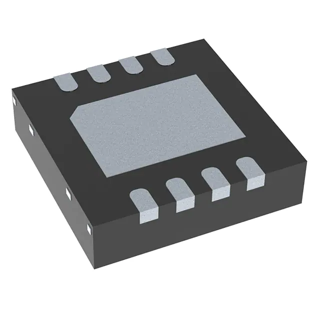
- Part No.:
- SE97TK,118
- Manufacturer:
- NXP Semiconductors
- Category:
- Thermal Management
- Package:
- 8-VFDFN Exposed Pad
- Datasheet:
-
 SE97TK,118.pdf
- Description:
- IC TEMP SENSOR DIMM 8-HVSON
- Quantity:
- Payment:

- Shipping:

Inventory:4,016
Please send an inquiry. Send us your inquiry, and we will respond immediately.
Product details
Overview
SE97TK,118 from NXP Semiconductors is a JEDEC JC-42.4-compliant DDR memory module temperature sensor with integrated 256-byte SPD EEPROM, operating from −40 °C to +125 °C with ±1 °C max accuracy between +75 °C and +95 °C, 11-bit ΔΣ ADC resolution (0.125 °C), and I²C/SMBus interface - deployed on SO-DIMM/RDIMM modules for DRAM case temperature estimation and thermal throttling control in thin-and-light notebooks.
For engineers reviewing the SE97TK,118 datasheet, SE97TK,118 pinout, SE97TK,118 application, or SE97TK,118 equivalent, key selection considerations include JEDEC Grade B thermal accuracy, programmable EVENT output polarity and hysteresis, dual-function EEPROM (PWP/RWP protection), SMBus TIMEOUT/ALERT support, and HVSON8 package compatibility with DDR3 RDIMM ECC and mobile platform memory modules.
Technical Context
The SE97TK,118 integrates a local temperature sensor and 256-byte serial EEPROM on a single die, sharing I²C/SMBus (0–400 kHz) with separate slave addresses (0x30 for temp sensor, 0x50 for EEPROM normal access, 0x30 for software write protect). Its 11-bit ΔΣ ADC performs conversions every 125 ms (8 Hz), latching results into a 16-bit temperature register with MSB-first data transfer.
Three address pins (A0–A2) enable up to eight devices per bus; A0 supports overvoltage-tolerant (10 V) software write protection. The open-drain EVENT output is configurable as active-HIGH/LOW comparator or interrupt, with independent critical/upper/lower trip points, hysteresis (0/1.5/3/6 °C), and lockable alarm bands - all controlled via a dedicated configuration register.
Key Specifications
| Parameter | Value and Actual Design Meaning |
|---|---|
| Temperature Range | −40 °C to +125 °C; enables full DDR3 DRAM thermal monitoring across industrial and extended commercial environments. |
| Accuracy (JEDEC B) | ±1 °C max from +75 °C to +95 °C; meets JC-42.4 TSE 2002B3 specification for DIMM thermal sensing reliability. |
| Resolution | 0.125 °C (11-bit ΔΣ ADC); supports fine-grained thermal throttling decisions without external signal conditioning. |
| EEPROM Size & Protection | 256 bytes (128 B PWP/RWP lower block + 128 B unprotected upper block); secures vendor SPD data while enabling runtime telemetry storage. |
| I²C/SMBus Speed | 0–400 kHz Fast-mode; compatible with standard motherboard SMBus controllers and allows burst reads during thermal event handling. |
| Supply Voltage | VDD = 3.0–3.6 V (sensor + EEPROM write); EEPROM read functional down to 1.7 V - ensures SPD data accessibility during low-power states. |
| Shutdown Current | 5.0 μA max; minimizes standby power impact on memory module power budget. |
Pinout & Package
SE97TK,118 uses the HVSON8 (SOT908-1) package: 3 mm × 3 mm × 0.85 mm, no leads, 8-terminal thermal-enhanced plastic body optimized for DIMM surface mounting and heat dissipation.
| Pin/Terminal | Circuit Role | Design Meaning |
|---|---|---|
| A0 | I²C slave address bit 0 | Internal pull-down; overvoltage tolerant to 10 V for software write-protection activation - enables secure SPD programming without hardware changes. |
| A1 | I²C slave address bit 1 | Internal pull-down; selects one of eight possible I²C addresses (0x30–0x37) on shared DIMM bus. |
| A2 | I²C slave address bit 2 | Internal pull-down; completes 3-bit hardware address selection for multi-sensor DIMM configurations. |
| VSS | Ground reference | Common return path for analog sensor and digital EEPROM; requires low-impedance PCB connection to minimize noise coupling. |
| SDA | I²C bidirectional data line | Open-drain I/O requiring external pull-up; transmits temperature data, EEPROM contents, and register writes/reads using MSB-first protocol. |
| SCL | I²C clock input | Open-drain input synchronized to host controller; supports SMBus TIMEOUT (25–35 ms) to prevent bus lockup during firmware hangs. |
| EVENT | Thermal alarm output | Open-drain output configurable as comparator (active HIGH/LOW) or interrupt; asserts on crossing critical/upper/lower thresholds - directly interfaces with chipset thermal management logic. |
| VDD | Power supply | 3.0–3.6 V supply powering both sensor and EEPROM; supports 1.7 V read-only operation for SPD access during low-voltage system states. |
Key Features
| Feature | Design Value |
|---|---|
| JEDEC JC-42.4 TSE 2002B3 compliance | Validated ±0.5 °C typical / ±1 °C max accuracy in +75 °C to +95 °C range - ensures interoperability with DDR3 RDIMM ECC and JEDEC-defined thermal throttling algorithms. |
| Configurable EVENT output modes | Three operational modes (comparator, interrupt, critical-only) with programmable polarity and hysteresis - enables direct integration into both thermostat-style fan control and microprocessor-driven dynamic throttling systems. |
| Dual-purpose 256-byte EEPROM | Lower 128 B supports Permanent/Reversible Write Protection (PWP/RWP); upper 128 B remains freely writable - satisfies SPD storage requirements while allowing runtime logging of thermal history or calibration data. |
| SMBus ALERT Response Address (ARA) | Default-enabled ARA (0x0C) allows EVENT signals from multiple SE97TK,118 devices to be wire-ANDed and resolved via bus arbitration - simplifies multi-DIMM thermal interrupt handling without additional GPIOs. |
| Single-die sensor + EEPROM integration | Monolithic construction eliminates inter-die thermal drift and improves long-term reliability versus discrete sensor+EEPROM solutions on memory modules. |
Applications
| DDR3 RDIMM Thermal Monitoring | Laptop DRAM Throttling Control |
|---|---|
|
Use Scenario: Mounted directly on DDR3 Registered DIMMs to measure local DRAM temperature and estimate Tcase for JEDEC-compliant thermal management. IC Role / Device Role / Timing Role: Local temperature sensor + SPD EEPROM providing real-time thermal feedback and memory module identity data to chipset. Use Value: Enables up to 30% improvement in thermal headroom for thin-and-light notebooks by replacing worst-case ambient estimates with actual DRAM junction temperature. |
Use Scenario: Integrated into SO-DIMM modules of ultrabooks and 2-in-1 convertibles to trigger dynamic memory traffic throttling based on measured temperature. IC Role / Device Role / Timing Role: Primary thermal sensor feeding temperature data to CPU memory controller for adaptive refresh rate scaling and bandwidth limiting. Use Value: Prevents DRAM overheating at 85 °C max operating temperature while maintaining performance under sustained workloads. |
| Enterprise Server Memory Modules | DDR2/DDR3 Memory SPD Replacement |
|
Use Scenario: Used on server-grade RDIMMs supporting ECC to provide redundant thermal sensing and fail-safe shutdown triggers. IC Role / Device Role / Timing Role: Critical temperature monitor with lockable alarm registers and non-volatile trip point storage - ensures consistent behavior across power cycles. Use Value: Supports high-availability requirements through hysteresis-configurable critical alarms and SMBus TIMEOUT resilience against bus faults. |
Use Scenario: Direct replacement for legacy Serial Presence Detect (SPD) EEPROMs with added temperature sensing capability on DDR2/DDR3 modules. IC Role / Device Role / Timing Role: Dual-function IC combining SPD data storage (vendor ID, timing parameters) and real-time thermal telemetry in same footprint. Use Value: Eliminates need for separate SPD and thermal sensor components, reducing BOM count and PCB area on memory modules. |
Equivalent & Alternatives
The following parts are listed as comparable options for similar temperature-sensing-with-SPD applications.
| Alternative Part | Technical Difference | Application Difference | Selection Advice |
|---|---|---|---|
| SE97PW,118 | TSSOP8 package (4.4 mm width); higher thermal resistance than HVSON8; identical electrical specs and register map. | Better suited for prototyping or legacy DIMM layouts with larger pad spacing; less optimal for space-constrained SO-DIMMs. | Select SE97PW,118 only when board layout cannot accommodate 3 mm × 3 mm HVSON8 footprint. |
| SE97TP,118 | HWSON8 package (2 mm × 3 mm × 0.8 mm); improved VPOR/EVENT IOL drive strength; otherwise functionally identical. | Preferred for next-generation ultra-thin DIMMs requiring lowest profile and enhanced noise immunity on EVENT line. | Choose SE97TP,118 when designing for JEDEC VCED-3 PSON8-compliant modules needing tighter voltage tolerance on EVENT assertion. |
Compared with SE97TK,118, SE97PW,118 offers mechanical compatibility at the cost of thermal performance, while SE97TP,118 delivers superior package miniaturization and drive capability - making SE97TK,118 the balanced choice for mainstream DDR3 RDIMM/ECC deployments where thermal enhancement and footprint efficiency are both critical.
Availability
SE97TK,118 is available at Aetrix Electronics and suitable for DDR3 RDIMM thermal monitoring, laptop DRAM throttling control, and enterprise server memory modules requiring stable component supply, JEDEC-compliant accuracy, and long-term SPD data integrity.
Supply support for SE97TK,118 includes scheduled delivery planning, volume procurement assistance, BOM continuity management, traceable sourcing, and lifecycle availability coordination for OEM customers, industrial embedded developers, connected-device designers, and electronics production programs.
Manufacturer
NXP Semiconductors is a global semiconductor leader focused on secure connectivity solutions for automotive, industrial, and communication infrastructure markets.
The SE97TK,118 belongs to NXP's JEDEC-compliant memory interface sensor family, designed specifically to meet JC-42.4 Mobile Platform Memory Module Temperature Sensor requirements for DDR2/DDR3 DIMMs with integrated SPD functionality.
FAQ
What is the primary application of the SE97TK,118?
The SE97TK,118 is primarily used as a JEDEC JC-42.4-compliant temperature sensor and SPD EEPROM on DDR3 RDIMM and SO-DIMM modules. It measures local DRAM temperature to enable accurate thermal throttling, replaces legacy SPD-only EEPROMs, and supports dynamic memory refresh scaling - all within a single HVSON8 package. Its design targets thin-and-light notebooks and enterprise servers requiring reliable, standards-aligned thermal management.
Does the SE97TK,118 support SMBus TIMEOUT and ALERT functions?
Yes, the SE97TK,118 fully supports SMBus TIMEOUT (default enabled, resets internal state if SCL held low 25–35 ms) and SMBus ALERT Response Address (ARA = 0x0C, default ON). These features prevent system lockups and allow multiple SE97TK,118 devices on one bus to share an interrupt line via wire-AND arbitration - critical for multi-DIMM platforms where bus resource efficiency matters.
How is EEPROM write protection implemented on the SE97TK,118?
The SE97TK,118 implements two-tier EEPROM write protection: the lower 128 bytes (00h–7Fh) support Permanent Write Protect (PWP) or Reversible Write Protect (RWP) via software command, securing SPD vendor data; the upper 128 bytes (80h–FFh) remain unprotected for runtime telemetry. A0 pin overvoltage tolerance (10 V) enables RWP activation without hardware modification - a feature confirmed in the official NXP SE97 datasheet Rev. 07.
What are the key differences between SE97TK,118 and SE97TP,118?
The SE97TK,118 uses HVSON8 (3 mm × 3 mm × 0.85 mm), while SE97TP,118 uses HWSON8 (2 mm × 3 mm × 0.8 mm) with improved VPOR/EVENT IOL drive strength. Both share identical register maps, thermal specs, and JEDEC compliance. SE97TP,118 is preferred for ultra-thin DIMMs needing minimal height and stronger interrupt signaling; SE97TK,118 balances thermal performance and manufacturability for mainstream DDR3 RDIMM applications.
Can the SE97TK,118 operate with VDD below 3.0 V?
Yes - the SE97TK,118 operates with VDD from 3.0 V to 3.6 V for full functionality (temperature sensing and EEPROM read/write), but EEPROM read operations remain functional down to 1.7 V. This allows SPD data retrieval during low-power or brown-out conditions while preserving thermal monitoring capability only above 3.0 V, as specified in the NXP SE97 product data sheet Rev. 07.
SE97TK,118 Specifications
- Product attributes
- Attribute value
- Manufacturer:
- NXP Semiconductors
- Series:
- -
- Package/Case:
- 8-VFDFN Exposed Pad
- Packaging:
- Tape & Reel (TR)
- Product Status:
- Obsolete
- Function:
- Temp Monitoring System (Sensor), DIMM DDR Memory
- Sensor Type:
- Internal
- Sensing Temperature:
- -40°C ~ 125°C
- Accuracy:
- ±3°C(Max)
- Topology:
- ADC (Sigma Delta), Comparator, Register Bank
- Output Type:
- I2C/SMBus
- Output Alarm:
- Yes
- Output Fan:
- Yes
- Voltage - Supply:
- 3V ~ 3.6V
- Operating Temperature:
- -40°C ~ 125°C
- Grade:
- -
- Qualification:
- -
- Mounting Type:
- Surface Mount
- Supplier Device Package:
- 8-HVSON (3x3)
SE97TK,118 FAQ
1.How can I place an order for SE97TK,118 through Aetrix?
Please submit a Request for Quotation (RFQ) for SE97TK,118 on Aetrix. Our sales agent will provide a competitive quotation and guide you through the order confirmation once you accept the terms.
2.Are the price and stock information for SE97TK,118 reliable?
The price and inventory of SE97TK,118 are updated periodically and may fluctuate due to market conditions. Stock and pricing data are typically refreshed every 24 hours. Quotation validity for SE97TK,118 is usually 5 days.
3.What payment methods are accepted for SE97TK,118?
We accept Wire Transfer, PayPal, Credit Card, Western Union, MoneyGram, and Escrow for SE97TK,118 transactions.
Note: Certain payment methods may incur a processing fee.
4.How is shipping managed for SE97TK,118?
SE97TK,118 orders can be shipped via leading logistics carriers, including DHL, UPS, FedEx, TNT, or Registered Mail.
Once your SE97TK,118 order is processed, you will receive an email with the shipment details and tracking number.
Note: Tracking information may take up to 24 hours to appear. Express delivery typically takes 3–5 business days.
5.How can I obtain technical support or documentation for SE97TK,118?
For technical support, including SE97TK,118 datasheets, pinout diagrams, or application guidance, please contact our engineering support team. They can provide detailed documentation and assistance for your SE97TK,118 requirements.
6.How does Aetrix verify that SE97TK,118 is sourced from the original manufacturer or authorized distributors?
All SE97TK,118 products on Aetrix are procured from qualified distributors and authorized channels. Our dedicated quality assurance team conducts strict verification, including traceability checks and, if necessary, third-party testing. This ensures that SE97TK,118 meets industry standards.
7.What is the process for return or replacement of SE97TK,118?
All SE97TK,118 units undergo pre-shipment inspection (PSI). If there is an issue with SE97TK,118, returns or replacements are accepted under the following conditions:
1.Quantity discrepancies, incorrect items, or visible external defects (such as breakage or corrosion), acknowledged by Aetrix.
2.The issue is reported within 90 days of delivery.
3.The SE97TK,118 part is unused and in its original packaging.
Return procedure for SE97TK,118:
1.Submit a request within 90 days.
2.Obtain a Return Material Authorization (RMA) from Aetrix.
SE97TK,118 Tags

-
EMC2101-ACZL-TR
Microchip Technology
-
MCP9844T-BE/MNY
Microchip Technology
-
EMC2101-R-ACZL-TR
Microchip Technology
-
MCP98244T-BE/MNY
Microchip Technology

-
TC670ECHTR
Microchip Technology

-
SE98ATP,547
NXP Semiconductors
-
AMC6821SDBQR
Texas Instruments

-
MAX6604AATA+T
Analog Devices Inc./Maxim Integrated
-
ADT7475ARQZ-REEL
onsemi
-
MAX6643LBBAEE+
Analog Devices Inc./Maxim Integrated

-
MAX6684ESA+T
Analog Devices Inc./Maxim Integrated
-
MAX6639AEE+
Analog Devices Inc./Maxim Integrated
Tech Hub

A practical engineering guide to 3.3V and 5V logic compatibility, input thresholds, resistor dividers, translator ICs, MOSFET level shifting, I2C pull-ups, timing limits and power-sequencing risks.

The 74HC595 uses push-pull logic outputs, while the TPIC6B595 uses 50 V open-drain DMOS sinks for higher-power loads. This guide compares timing, current limits, 3.3 V interfacing, load wiring, thermal…

The 74HC595 converts serial data into eight stable parallel outputs. This guide covers pin functions, shift and storage timing, OE and MR behavior, drive-current limits, cascading, voltage compatibilit…

A technical comparison of level-sensitive latches and edge-triggered flip-flops, covering timing windows, setup and hold limits, master–slave operation, time borrowing, race-through, HDL inference and…

A D latch stores one bit while Enable controls when data can pass. This reference covers gate-level operation, truth tables, transparency, setup and hold timing, LE versus OE, common ICs and practical …

An SR latch stores one bit through cross-coupled feedback. This engineering reference covers NOR and NAND implementations, truth tables, forbidden-state recovery, gated operation, switch debouncing, fa…

Latch circuits retain one bit through feedback. This technical reference covers SR and D latches, truth tables, transparency, timing limits, latch-versus-flip-flop behavior, applications and common log…

An engineering guide to LED driver operation, constant-current and constant-voltage outputs, linear and switching topologies, dimming, IC selection, calculations, replacement compatibility, and fault c…

Operational amplifier guide covering op amp basics, feedback, ideal vs real op amps, common configurations, buffer circuits, offset, bias current, gain-bandwidth, slew rate, rail-to-rail limits and sel…

Jumper cables guide covering safe connection order, red and black clamp placement, final ground connection, cable gauge, length, clamp quality, copper vs CCA cables, jump starter comparison and battery…


