
 My Inquiry
 My Account


Skyworks Solutions Inc. SI5017-D-GMR
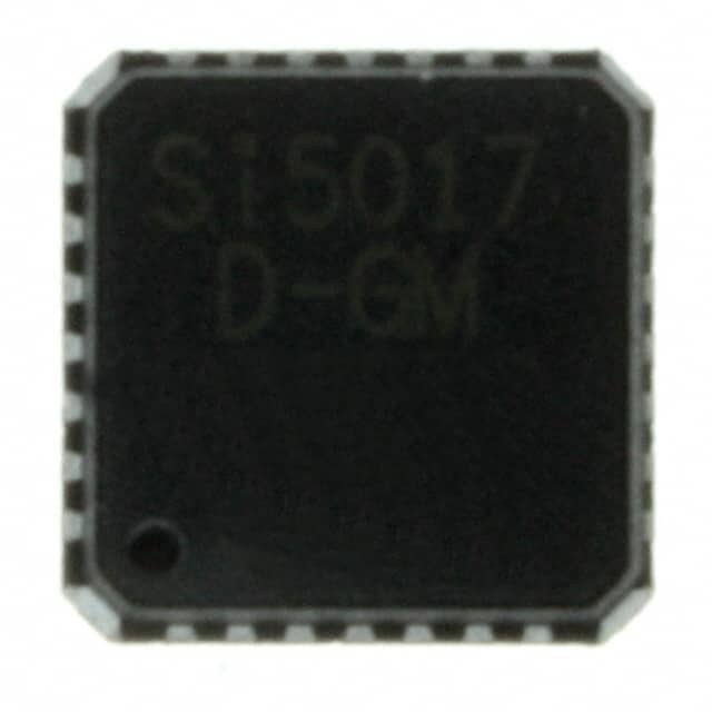
- Part No.:
- SI5017-D-GMR
- Manufacturer:
- Skyworks Solutions Inc.
- Category:
- Application Specific Clock/Timing
- Package:
- 28-VFQFN Exposed Pad
- Datasheet:
-
 SI5017-D-GMR.pdf
- Description:
- IC CLOCK/DATA RECOVERY 28MLP
- Quantity:
- Payment:

- Shipping:

Inventory:4,760
Please send an inquiry. Send us your inquiry, and we will respond immediately.
Product details
Overview
SI5017-D-GMR from Silicon Laboratories is a fully integrated OC-48/STM-16 SONET/SDH clock and data recovery (CDR) IC with integrated limiting amplifier, operating at 2.4–2.7 Gbps with 3.0 mUIrms typical jitter generation, 528 mW typical power dissipation, and 3.3 V supply. It serves as the core timing retimer in optical line cards and transceiver modules.
For engineers reviewing the SI5017-D-GMR datasheet, SI5017-D-GMR pinout, SI5017-D-GMR application, or SI5017-D-GMR equivalent, this page delivers verified functional identity, DSPLL™ architecture details, differential CML I/O behavior, loss-of-signal and BER alarm configuration, and validated alternative parts for SONET/SDH CDR substitution.
Technical Context
The SI5017-D-GMR implements a digital signal processing–based DSPLL™ to replace analog loop filters, enabling jitter generation of ≤3.0 mUIrms and jitter tolerance exceeding Bellcore GR-253-CORE masks. Its limiting amplifier accepts 10–1000 mVPP differential input swing and supports both reference-less and external reference (19.44–168.75 MHz) operation.
It delivers synchronous CML outputs: DOUT± and CLKOUT± with 700–900 mVPP swing into 100 Ω, 80–110 ps rise/fall times, and programmable slicing level (±15 mV offset), LOS threshold (0–40 mVPP), and BER alarm threshold (10−10 to 10−6).
Key Specifications
| Parameter | Value and Actual Design Meaning |
|---|---|
| Data Rate | 2.4–2.7 Gbps - supports OC-48/STM-16 (2.488 Gbps) and FEC-enhanced 2.7 Gbps links. |
| Jitter Generation | 3.0 mUIrms typ - meets SONET/SDH GR-253-CORE jitter specs without external filtering. |
| Supply Voltage | 3.3 V ±5% - internally regulated to 2.5 V; enables direct integration into 3.3 V telecom systems. |
| Differential Input Sensitivity | 10 mVPP min - recovers data from low-amplitude TIA outputs without external amplification. |
| Output Interface | CML - provides 700–900 mVPP differential swing into 100 Ω loads for direct connection to FPGA SerDes or laser drivers. |
| Reference Flexibility | Reference-less or 19.44–168.75 MHz external REFCLK - auto-detects 1/16, 1/32, or 1/128 VCO division ratio. |
| Alarm Functions | LOS, LOL, BER_ALM, LTR - configurable thresholds via analog voltage inputs (LOS_LVL, BER_LVL, SLICE_LVL). |
Pinout & Package
SI5017-D-GMR is housed in a 28-pin 5 × 5 mm micro leaded package (MLP) with exposed GND pad. Pin assignments are validated per Si5017-DS12 Rev. 1.2, Figure 15 and Table 8.
| Pin/Terminal | Circuit Role | Design Meaning |
|---|---|---|
| VDD (Pins 1,2,11,14,18,21,25) | Power supply | 3.3 V supply input; seven dedicated pins ensure low-impedance delivery for high-speed analog/RF sections. |
| DIN+, DIN– (Pins 12,13) | Differential data input | Accepts 10–1000 mVPP ac-coupled serial data; internal 100 Ω termination enables direct TIA interface. |
| REFCLK+, REFCLK– (Pins 5,6) | Optional reference clock input | Configures DSPLL center frequency; tied to VDD/GND for reference-less mode. |
| DOUT+, DOUT– (Pins 9,10) | Recovered data output | CML output with 700–900 mVPP swing; supports data squelch via DSQLCH pin. |
| CLKOUT+, CLKOUT– (Pins 22,23) | Recovered clock output | CML clock output synchronized to DOUT; disableable via CLK_DSBL pin. |
| LOS_LVL, BER_LVL, SLICE_LVL (Pins 3,4,20) | Analog control inputs | Set LOS threshold (0–40 mVPP), BER alarm level (10−10–10−6), and slicing offset (±15 mV). |
| RESET/CAL (Pin 16) | Calibration trigger | Initiates DSPLL loop gain calibration on falling edge; required for optimal jitter performance after power-up. |
Key Features
| Feature | Design Value |
|---|---|
| DSPLL™ architecture | Digital loop filter eliminates external components, reduces board-level noise sensitivity, and ensures stable jitter performance across temperature. |
| Programmable slicing level | ±15 mV adjustment via SLICE_LVL pin enables real-time BER optimization in production test and field deployment. |
| Loss-of-signal detection | Adjustable 0–40 mVPP threshold with hysteresis support prevents false alarms during marginal signal conditions. |
| Bit-error-rate monitoring | Proprietary algorithm generates BER_ALM when observed error rate exceeds user-set threshold (10−10 to 10−6). |
| Lock-to-reference (LTR) mode | Forces stable CLKOUT during LOS/LOL by locking to REFCLK or holding last VCO frequency-critical for system fault containment. |
Applications
| SONET/SDH Add/Drop Multiplexer | Optical Transceiver Module |
|---|---|
|
Use Scenario: Receives degraded OC-48 signals from fiber spans and regenerates clean data/clock for switching fabric. IC Role / Device Role / Timing Role: CDR retimer with limiting amplifier restores signal integrity prior to cross-connect switching. Use Value: 3.0 mUIrms jitter generation and 10 mVPP sensitivity enable reliable recovery after multiple amplification stages. |
Use Scenario: Embedded in SFP/SFF modules to recover clock/data from PIN/TIA outputs before serialization. IC Role / Device Role / Timing Role: High-sensitivity LA+CDR front-end providing jitter-clean CML outputs to laser driver or serializer. Use Value: 5×5 mm MLP footprint and single 3.3 V supply simplify module layout and reduce BOM count vs. discrete solutions. |
| SONET/SDH Regenerator | Test Equipment Signal Analyzer |
|
Use Scenario: Re-times long-haul OC-48 signals suffering accumulated jitter and amplitude distortion. IC Role / Device Role / Timing Role: Jitter-tolerant CDR with >40 UIPP tolerance at 600 Hz meets GR-253-CORE regeneration requirements. Use Value: Reference-less operation eliminates need for ultra-stable external clock, reducing cost and board space. |
Use Scenario: Used in bit-error-rate testers to validate transmitter compliance under stressed jitter conditions. IC Role / Device Role / Timing Role: Programmable BER monitor and slicing level control enable precise error thresholding and margin testing. Use Value: Analog-configurable LOS_LVL and BER_LVL pins allow rapid test setup without firmware changes. |
Equivalent & Alternatives
The following parts are listed as comparable options for similar CDR applications.
| Alternative Part | Technical Difference | Application Difference | Selection Advice |
|---|---|---|---|
| MAX3865E | 2.5 Gbps max rate; requires external loop filter; 4.5 mUIrms jitter gen; 5 V supply only. | Limited to non-FEC OC-48; higher power (1.2 W); incompatible with 3.3 V systems. | Select MAX3865E only if legacy 5 V infrastructure exists and FEC support is unnecessary. |
| LMH0341 | 2.97 Gbps max; no integrated limiting amplifier; requires external LA; 3.3 V supply; 3.5 mUIrms. | Needs discrete LA stage; larger total solution size; lacks BER monitoring and slicing control. | Choose LMH0341 when system already includes high-performance LA and only CDR function is needed. |
Compared with SI5017-D-GMR, MAX3865E offers lower integration and higher jitter, while LMH0341 shifts LA design burden to the system but supports higher data rates-neither matches SI5017-D-GMR's combined 2.7 Gbps FEC readiness, DSPLL jitter performance, and analog configurability in a 5×5 mm package.
Availability
SI5017-D-GMR is available at Aetrix Electronics and suitable for SONET/SDH add/drop multiplexers, optical transceiver modules, and telecom test equipment requiring stable component supply, long-term lifecycle assurance, and traceable sourcing.
Supply support for SI5017-D-GMR includes scheduled delivery planning, volume procurement assistance, BOM continuity management, traceable sourcing, and lifecycle availability coordination for OEM customers, industrial embedded developers, connected-device designers, and electronics production programs.
Manufacturer
Silicon Laboratories is a fabless semiconductor company specializing in precision timing, wireless, and mixed-signal ICs for communications, computing, and industrial markets.
The SI5017-D-GMR belongs to Silicon Labs' high-speed timing product line, designed specifically for SONET/SDH OC-48/STM-16 infrastructure where low jitter, small footprint, and integrated LA+CDR functionality are critical.
FAQ
What is the maximum supported data rate for SI5017-D-GMR?
The SI5017-D-GMR supports up to 2.7 Gbps, covering standard OC-48/STM-16 (2.488 Gbps) and forward error correction (FEC)-enhanced links. This capability is confirmed in the Electrical Specifications table (Table 3) and Functional Description section of the Si5017-DS12 datasheet Rev. 1.2, where fCLK is specified from 2.4 to 2.7 GHz.
Does SI5017-D-GMR require an external reference clock?
No, SI5017-D-GMR operates in reference-less mode by default-tying REFCLK+ to VDD and REFCLK– to GND configures autonomous CDR. An external reference (19.44–168.75 MHz) is optional and reduces acquisition time; the device auto-detects division ratio (1/16, 1/32, or 1/128). This dual-mode flexibility is documented in the "Operation Without an External Reference" and "Operation With an External Reference" sections.
How is loss-of-signal (LOS) threshold configured on SI5017-D-GMR?
The LOS threshold is set by applying a voltage (1.0–2.5 V) to the LOS_LVL pin (Pin 3), which maps linearly to a 0–40 mVPP differential input threshold per Equation in Table 3 and Figure 6. Grounding LOS_LVL disables LOS detection. This analog programming method allows field-adjustable sensitivity without firmware updates.
What output interface does SI5017-D-GMR use for recovered clock and data?
SI5017-D-GMR uses current-mode logic (CML) outputs for both DOUT± (Pins 9,10) and CLKOUT± (Pins 22,23), delivering 700–900 mVPP differential swing into 100 Ω loads. Rise/fall times are 70–110 ps, and outputs support clock disable (CLK_DSBL) and data squelch (DSQLCH) functions per the Functional Block Diagram and Pin Descriptions.
What is the role of the REXT pin on SI5017-D-GMR?
The REXT pin (Pin 19) connects to a 10 kΩ (1%) resistor to ground to set internal bias currents. This external resistor enables precise current generation, reducing power consumption versus internal resistor methods. The requirement is explicitly stated in the "Bias Generation Circuitry" section and validated in the Typical Application Schematic (page 11).
SI5017-D-GMR Specifications
- Product attributes
- Attribute value
- Manufacturer:
- Skyworks Solutions Inc.
- Series:
- DSPLL®
- Package/Case:
- 28-VFQFN Exposed Pad
- Packaging:
- Tape & Reel (TR)
- Product Status:
- Active
- Programmable:
- Not Verified
- PLL:
- Yes
- Main Purpose:
- SONET/SDH, ATM applications
- Input:
- Clock
- Output:
- CML
- Number of Circuits:
- 1
- Ratio - Input:Output:
- 1:2
- Differential - Input:Output:
- Yes/Yes
- Frequency - Max:
- 2.7GHz
- Voltage - Supply:
- 3.135V ~ 3.465V
- Operating Temperature:
- -40°C ~ 85°C
- Mounting Type:
- Surface Mount
- Grade:
- -
- Qualification:
- -
- Supplier Device Package:
- 28-MLP (5x5)
SI5017-D-GMR FAQ
1.How can I place an order for SI5017-D-GMR through Aetrix?
Please submit a Request for Quotation (RFQ) for SI5017-D-GMR on Aetrix. Our sales agent will provide a competitive quotation and guide you through the order confirmation once you accept the terms.
2.Are the price and stock information for SI5017-D-GMR reliable?
The price and inventory of SI5017-D-GMR are updated periodically and may fluctuate due to market conditions. Stock and pricing data are typically refreshed every 24 hours. Quotation validity for SI5017-D-GMR is usually 5 days.
3.What payment methods are accepted for SI5017-D-GMR?
We accept Wire Transfer, PayPal, Credit Card, Western Union, MoneyGram, and Escrow for SI5017-D-GMR transactions.
Note: Certain payment methods may incur a processing fee.
4.How is shipping managed for SI5017-D-GMR?
SI5017-D-GMR orders can be shipped via leading logistics carriers, including DHL, UPS, FedEx, TNT, or Registered Mail.
Once your SI5017-D-GMR order is processed, you will receive an email with the shipment details and tracking number.
Note: Tracking information may take up to 24 hours to appear. Express delivery typically takes 3–5 business days.
5.How can I obtain technical support or documentation for SI5017-D-GMR?
For technical support, including SI5017-D-GMR datasheets, pinout diagrams, or application guidance, please contact our engineering support team. They can provide detailed documentation and assistance for your SI5017-D-GMR requirements.
6.How does Aetrix verify that SI5017-D-GMR is sourced from the original manufacturer or authorized distributors?
All SI5017-D-GMR products on Aetrix are procured from qualified distributors and authorized channels. Our dedicated quality assurance team conducts strict verification, including traceability checks and, if necessary, third-party testing. This ensures that SI5017-D-GMR meets industry standards.
7.What is the process for return or replacement of SI5017-D-GMR?
All SI5017-D-GMR units undergo pre-shipment inspection (PSI). If there is an issue with SI5017-D-GMR, returns or replacements are accepted under the following conditions:
1.Quantity discrepancies, incorrect items, or visible external defects (such as breakage or corrosion), acknowledged by Aetrix.
2.The issue is reported within 90 days of delivery.
3.The SI5017-D-GMR part is unused and in its original packaging.
Return procedure for SI5017-D-GMR:
1.Submit a request within 90 days.
2.Obtain a Return Material Authorization (RMA) from Aetrix.
SI5017-D-GMR Tags
-
LMK00334RTVRQ1
Texas Instruments
.jpg)
-
DSC557-0344FI0T
Microchip Technology
-
9FGV0241AKILFT
Renesas

-
9DBL0452CKILFT
Renesas
-
DSC557-0344FL1T
Microchip Technology
-
RC19008AGND#KB0
Renesas
-
RC19008AGND#BB0
Renesas

-
9DB403DGILFT
Renesas
-
9DB233AGILFT
Renesas

-
9DB803DGILFT
Renesas
-
9FGL0851DKILFT
Renesas
-
AB-557-03-HCHC-F-L-C-T
Abracon LLC
Tech Hub

Counterfeit components can hide behind convincing markings and passing basic function tests. This engineering reference covers source traceability, external inspection, X-ray, XRF, electrical testing, …

A practical engineering and sourcing framework covering lifecycle verification, lifetime-buy calculations, replacement qualification, supplier checks and counterfeit-risk controls.

TTL and CMOS logic families differ in thresholds, loading, output drive, power and timing. This engineering guide compares 74HC and 74HCT, calculates noise margins and checks 3.3 V/5 V compatibility.

A practical engineering guide to 3.3V and 5V logic compatibility, input thresholds, resistor dividers, translator ICs, MOSFET level shifting, I2C pull-ups, timing limits and power-sequencing risks.

The 74HC595 uses push-pull logic outputs, while the TPIC6B595 uses 50 V open-drain DMOS sinks for higher-power loads. This guide compares timing, current limits, 3.3 V interfacing, load wiring, thermal…

The 74HC595 converts serial data into eight stable parallel outputs. This guide covers pin functions, shift and storage timing, OE and MR behavior, drive-current limits, cascading, voltage compatibilit…

A technical comparison of level-sensitive latches and edge-triggered flip-flops, covering timing windows, setup and hold limits, master–slave operation, time borrowing, race-through, HDL inference and…

A D latch stores one bit while Enable controls when data can pass. This reference covers gate-level operation, truth tables, transparency, setup and hold timing, LE versus OE, common ICs and practical …

An SR latch stores one bit through cross-coupled feedback. This engineering reference covers NOR and NAND implementations, truth tables, forbidden-state recovery, gated operation, switch debouncing, fa…

Latch circuits retain one bit through feedback. This technical reference covers SR and D latches, truth tables, transparency, timing limits, latch-versus-flip-flop behavior, applications and common log…


