
 My Inquiry
 My Account


Skyworks Solutions Inc. SI5018-BM
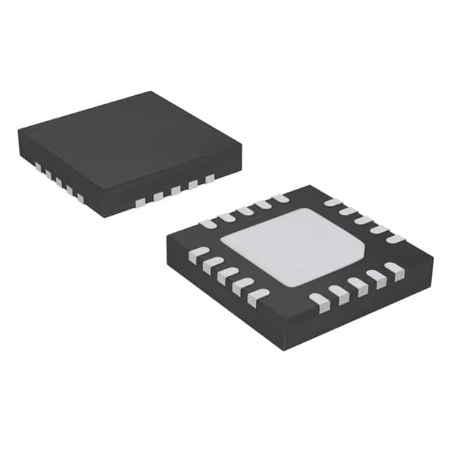
- Part No.:
- SI5018-BM
- Manufacturer:
- Skyworks Solutions Inc.
- Category:
- Application Specific Clock/Timing
- Package:
- 20-VFQFN Exposed Pad
- Datasheet:
-
 SI5018-BM.pdf
- Description:
- IC CLOCK/DATA RECOVERY LP 20QFN
- Quantity:
- Payment:

- Shipping:

Inventory:1,134
Please send an inquiry. Send us your inquiry, and we will respond immediately.
Product details
Overview
SI5018-BM from Silicon Laboratories is a fully-integrated clock and data recovery (CDR) IC for OC-48/STM-16 (2.488 GHz) and FEC-enhanced 2.7 Gbps serial links. It performs timing extraction and data retiming using DSPLL™ technology, delivers 2.9 mUIrms jitter generation, operates from a single 2.5 V supply, and supports industrial temperature range (–40 to 85 °C). It is deployed in optical transceiver modules and SONET/SDH regenerators.
For engineers reviewing the SI5018-BM datasheet, SI5018-BM pinout, SI5018-BM application, or SI5018-BM equivalent, key selection criteria include jitter compliance with Bellcore GR-253-CORE, DSPLL™ self-calibration behavior, CML output drive capability, REXT bias resistor requirement, and loss-of-lock (LOL) alarm functionality under reference clock absence.
Technical Context
The SI5018-BM implements a digital signal processing (DSP)-based DSPLL™ architecture that replaces analog loop filter components, eliminating board-level noise coupling paths and enabling guaranteed SONET/SDH jitter compliance. Its PLL uses a divided-down VCO output compared to REFCLK to detect lock status, with LOL assertion triggered at ±600 ppm frequency deviation.
It supports dual-mode operation: standard OC-48/STM-16 (2.488 GHz) and FEC-enabled 2.7 Gbps mode, where reference clock selection (19.44 MHz, 83.31 MHz, or 166.63 MHz) determines VCO centering via 128×, 32×, or 16× multiplication. Input termination accommodates both differential and single-ended DIN/REFCLK drive, with 100 Ω differential input impedance and 200–1500 mVPP differential swing support.
Key Specifications
| Parameter | Value and Actual Design Meaning |
|---|---|
| Supply Voltage | 2.5 V ±5% - Enables single-rail power design; requires stable low-noise 2.5 V source with ≤122 mA draw. |
| Data Rate Support | 2.488 GHz (OC-48/STM-16) and 2.7 GHz (FEC) - Directly targets SONET/SDH line rates with forward error correction compatibility. |
| Jitter Generation | 2.9 mUIrms (typ) - Meets and exceeds Bellcore GR-253-CORE requirements for recovered clock/data outputs. |
| Power Dissipation | 270 mW (typ at OC-48) - Enables thermal management in dense optical module layouts with ϕJA = 38 °C/W. |
| Input Impedance | 100 Ω differential (DIN/REFCLK) - Matches standard 50 Ω trace + 50 Ω termination for minimal reflection. |
| Output Interface | CML (DOUT/CLKOUT) - Provides 780–1260 mVPP differential swing into 100 Ω loads for high-speed interconnects. |
| Reference Clock Range | 19.44–168.75 MHz - Supports three VCO multiplication ratios (16×/32×/128×) for automatic REFCLK detection. |
Pinout & Package
The SI5018-BM is housed in a 4×4 mm, 20-pin micro leadframe package (MLP) with exposed thermal pad. The package features 16 signal terminals and 4 dedicated VDD/GND pins plus bottom-side GND pad for low-inductance grounding.
| Pin/Terminal | Circuit Role | Design Meaning |
|---|---|---|
| 1 | REXT | Bias current reference - Requires external 10 kΩ (1%) resistor to GND to set internal current sources and minimize power. |
| 4–5 | REFCLK+, REFCLK– | Differential reference clock input - Sets VCO center frequency; enables automatic ratio detection (16×/32×/128×). |
| 6 | LOL | LVTTL loss-of-lock indicator - Asserts high when recovered clock deviates >±600 ppm from REFCLK; not active during PWRDN/CAL. |
| 9–10 | DIN+, DIN– | Differential high-speed data input - Accepts 200–1500 mVPP swing; supports AC- or DC-coupled termination per application. |
| 12–13 | DOUT–, DOUT+ | CML differential data output - Retimed data aligned to CLKOUT rising edge; 780–1260 mVPP into 100 Ω load. |
| 15 | PWRDN/CAL | Multi-function LVTTL input - High = output driver shutdown; falling edge initiates DSPLL™ self-calibration. |
| 16–17 | CLKOUT–, CLKOUT+ | CML differential clock output - Recovered clock derived from DIN; defaults to REFCLK-derived clock when no data present. |
| 2, 7, 11, 14 | VDD | 2.5 V supply - Four dedicated power pins reduce IR drop and improve PSRR in high-frequency operation. |
| 3, 8, 18–20 + GND Pad | GND | Ground reference - Bottom thermal pad must be connected directly to analog ground plane for thermal and noise performance. |
Key Features
| Feature | Design Value |
|---|---|
| DSPLL™ architecture | Eliminates external loop filter components, removing critical noise injection points and ensuring robust jitter performance across PCB stackups. |
| Automatic REFCLK detection | Identifies 19.44 MHz, 83.31 MHz, or 166.63 MHz reference clocks and configures VCO multiplication ratio (128×/32×/16×) without external programming. |
| Integrated bias control | Uses external 10 kΩ REXT to precisely set internal bias currents, reducing power vs. on-die resistor solutions and improving process/voltage/temp stability. |
| Loss-of-lock monitoring | Provides real-time LOL status based on measured frequency deviation between divided VCO and REFCLK, supporting system fault diagnostics. |
| Powerdown with calibration trigger | Single PWRDN/CAL pin enables output shutdown for redundancy and initiates DSPLL™ self-calibration on falling edge for consistent lock behavior. |
Applications
| Optical Transceiver Modules | SONET/SDH Regenerators |
|---|---|
Use Scenario: Embedded in SFP/SFF modules to recover clock and data from 2.488 Gbps optical signals before retiming and driving laser drivers or TIAs. IC Role / Device Role / Timing Role: CDR core performing jitter cleanup, phase alignment, and low-jitter clock regeneration for downstream serializer/deserializer stages. Use Value: Achieves <3.0 mUIrms jitter generation, meeting GR-253-CORE mask requirements without external filtering or tuning. |
Use Scenario: Installed in line cards of SONET/SDH regenerators to restore timing integrity after long-haul fiber transmission with accumulated jitter. IC Role / Device Role / Timing Role: Primary clock recovery element extracting clean timing from degraded OC-48 serial streams and retransmitting regenerated data/clock. Use Value: Exceeds Bellcore/ITU-T G.958 jitter tolerance and transfer specifications, enabling reliable multi-node network cascading. |
| Add/Drop Multiplexers | SONET/SDH Test Equipment |
Use Scenario: Used in ADM backplane interfaces to synchronize tributary data streams entering/exiting the multiplexer fabric. IC Role / Device Role / Timing Role: Interface CDR providing deterministic latency and phase-aligned DOUT/CLKOUT for time-sensitive switching logic. Use Value: Fixed 225–270 ps clock-to-data delay (tC-D) ensures predictable setup/hold timing margins for FPGA-based switch fabric control. |
Use Scenario: Integrated into bit-error-rate testers (BERTs) and jitter analyzers to validate OC-48/STM-16 device compliance under stressed conditions. IC Role / Device Role / Timing Role: Reference CDR generating ultra-low-jitter outputs used as golden clocks for measurement instrumentation calibration. Use Value: 2.9 mUIrms jitter generation enables sub-mUI resolution in jitter spectrum analysis and mask testing. |
Equivalent & Alternatives
The following parts are listed as comparable options for similar clock and data recovery applications.
| Alternative Part | Technical Difference | Application Difference | Selection Advice |
|---|---|---|---|
| MAX3875E | Requires external loop filter components; higher typical power (450 mW); supports only OC-48 (no FEC mode). | Limited to legacy SONET systems without FEC; less immune to board-level noise due to analog PLL architecture. | Choose when existing designs use MAXIM's evaluation platforms or require pin-compatible upgrade path from older MAX3875 variants. |
| ICS872002 | Fixed 2.488 GHz operation only; no REFCLK auto-detection; LVTTL/CMOS outputs instead of CML; higher jitter (4.2 mUIrms). | Suitable for cost-sensitive non-regenerator applications where full Bellcore compliance is not mandated. | Prefer for simpler, lower-cost CDR needs in non-critical timing roles where DSPLL™ advantages are unnecessary. |
Compared with MAX3875E and ICS872002, the SI5018-BM provides superior jitter performance, eliminates external loop filter design complexity, supports FEC-enhanced 2.7 Gbps operation, and enables automatic reference clock configuration-making it optimal for next-generation optical infrastructure requiring guaranteed compliance and layout flexibility.
Availability
SI5018-BM is available at Aetrix Electronics and suitable for optical transceiver modules, SONET/SDH regenerators, and add/drop multiplexers requiring stable component supply across extended temperature ranges and long production lifecycles.
Supply support for SI5018-BM includes scheduled delivery planning, volume procurement assistance, BOM continuity management, traceable sourcing, and lifecycle availability coordination for OEM customers, industrial embedded developers, connected-device designers, and electronics production programs.
Manufacturer
Silicon Laboratories is a fabless semiconductor company specializing in precision timing, wireless, and mixed-signal ICs for communications, computing, and industrial markets.
The SI5018-BM belongs to Silicon Labs' SiPHY™ family of high-speed CDRs, engineered specifically for SONET/SDH optical infrastructure where low jitter, small footprint, and single-supply operation are critical design constraints.
FAQ
What is the primary function of the SI5018-BM in a SONET/SDH system?
The SI5018-BM serves as a clock and data recovery IC that extracts precise timing information and retimes serial data from OC-48/STM-16 (2.488 GHz) or FEC-enhanced 2.7 Gbps inputs. In a SONET/SDH system, it ensures jitter-clean clock and data outputs compliant with Bellcore GR-253-CORE, enabling reliable signal regeneration and synchronization. The SI5018-BM achieves this using DSPLL™ technology and integrated CML drivers.
How does the SI5018-BM handle reference clock detection and configuration?
The SI5018-BM automatically detects whether the applied REFCLK is 19.44 MHz, 83.31 MHz, or 166.63 MHz and configures its internal VCO multiplication ratio accordingly (128×, 32×, or 16×). This eliminates manual configuration or external strapping. The SI5018-BM uses continuous monitoring of REFCLK frequency to center the VCO output between 2.488 GHz and 2.7 GHz, ensuring correct operation across all supported modes.
What is the role of the REXT pin on the SI5018-BM, and what value resistor is required?
The REXT pin on the SI5018-BM connects to an external 10 kΩ (1%) resistor tied to GND, which sets internal bias currents for optimal power efficiency and process/voltage/temperature stability. This external biasing reduces power versus on-die resistors and improves repeatability. Omitting or misvaluing the REXT resistor causes incorrect biasing, increased power consumption, and potential jitter degradation in the SI5018-BM.
Does the SI5018-BM support both differential and single-ended input drive for DIN and REFCLK?
Yes, the SI5018-BM supports both differential and single-ended drive for DIN+/- and REFCLK+/- inputs. When driven single-endedly, the active input must exceed 200 mVPP differential swing, and the unused input must be AC-coupled to ground. For differential drive, the voltage difference between pins must exceed 200 mVPP. Both configurations maintain full 100 Ω input impedance and jitter performance in the SI5018-BM.
What happens to the LOL (Loss-of-Lock) output when the REFCLK signal is removed?
When REFCLK is removed, the LOL output of the SI5018-BM is asserted high to indicate unknown lock status, as the PLL cannot compare recovered clock frequency to a reference. This differs from normal out-of-lock conditions (triggered by >±600 ppm deviation), where LOL toggles during reacquisition attempts. The SI5018-BM does not assert LOL during PWRDN/CAL activation, preserving diagnostic clarity.
SI5018-BM Specifications
- Product attributes
- Attribute value
- Manufacturer:
- Skyworks Solutions Inc.
- Series:
- SiPHY™, DSPLL®
- Package/Case:
- 20-VFQFN Exposed Pad
- Packaging:
- Tube
- Product Status:
- Obsolete
- Programmable:
- Not Verified
- PLL:
- Yes
- Main Purpose:
- SONET/SDH, ATM applications
- Input:
- Clock
- Output:
- CML
- Number of Circuits:
- 1
- Ratio - Input:Output:
- 1:2
- Differential - Input:Output:
- Yes/Yes
- Frequency - Max:
- 2.7GHz
- Voltage - Supply:
- 2.375V ~ 2.625V
- Operating Temperature:
- -40°C ~ 85°C
- Mounting Type:
- Surface Mount
- Grade:
- -
- Qualification:
- -
- Supplier Device Package:
- 20-QFN (4x4)
SI5018-BM FAQ
1.How can I place an order for SI5018-BM through Aetrix?
Please submit a Request for Quotation (RFQ) for SI5018-BM on Aetrix. Our sales agent will provide a competitive quotation and guide you through the order confirmation once you accept the terms.
2.Are the price and stock information for SI5018-BM reliable?
The price and inventory of SI5018-BM are updated periodically and may fluctuate due to market conditions. Stock and pricing data are typically refreshed every 24 hours. Quotation validity for SI5018-BM is usually 5 days.
3.What payment methods are accepted for SI5018-BM?
We accept Wire Transfer, PayPal, Credit Card, Western Union, MoneyGram, and Escrow for SI5018-BM transactions.
Note: Certain payment methods may incur a processing fee.
4.How is shipping managed for SI5018-BM?
SI5018-BM orders can be shipped via leading logistics carriers, including DHL, UPS, FedEx, TNT, or Registered Mail.
Once your SI5018-BM order is processed, you will receive an email with the shipment details and tracking number.
Note: Tracking information may take up to 24 hours to appear. Express delivery typically takes 3–5 business days.
5.How can I obtain technical support or documentation for SI5018-BM?
For technical support, including SI5018-BM datasheets, pinout diagrams, or application guidance, please contact our engineering support team. They can provide detailed documentation and assistance for your SI5018-BM requirements.
6.How does Aetrix verify that SI5018-BM is sourced from the original manufacturer or authorized distributors?
All SI5018-BM products on Aetrix are procured from qualified distributors and authorized channels. Our dedicated quality assurance team conducts strict verification, including traceability checks and, if necessary, third-party testing. This ensures that SI5018-BM meets industry standards.
7.What is the process for return or replacement of SI5018-BM?
All SI5018-BM units undergo pre-shipment inspection (PSI). If there is an issue with SI5018-BM, returns or replacements are accepted under the following conditions:
1.Quantity discrepancies, incorrect items, or visible external defects (such as breakage or corrosion), acknowledged by Aetrix.
2.The issue is reported within 90 days of delivery.
3.The SI5018-BM part is unused and in its original packaging.
Return procedure for SI5018-BM:
1.Submit a request within 90 days.
2.Obtain a Return Material Authorization (RMA) from Aetrix.
SI5018-BM Tags
-
LMK00334RTVRQ1
Texas Instruments
.jpg)
-
DSC557-0344FI0T
Microchip Technology
-
9FGV0241AKILFT
Renesas

-
9DBL0452CKILFT
Renesas
-
DSC557-0344FL1T
Microchip Technology
-
RC19008AGND#KB0
Renesas
-
RC19008AGND#BB0
Renesas

-
9DB403DGILFT
Renesas
-
9DB233AGILFT
Renesas

-
9DB803DGILFT
Renesas
-
9FGL0851DKILFT
Renesas
-
AB-557-03-HCHC-F-L-C-T
Abracon LLC
Tech Hub

Counterfeit components can hide behind convincing markings and passing basic function tests. This engineering reference covers source traceability, external inspection, X-ray, XRF, electrical testing, …

A practical engineering and sourcing framework covering lifecycle verification, lifetime-buy calculations, replacement qualification, supplier checks and counterfeit-risk controls.

TTL and CMOS logic families differ in thresholds, loading, output drive, power and timing. This engineering guide compares 74HC and 74HCT, calculates noise margins and checks 3.3 V/5 V compatibility.

A practical engineering guide to 3.3V and 5V logic compatibility, input thresholds, resistor dividers, translator ICs, MOSFET level shifting, I2C pull-ups, timing limits and power-sequencing risks.

The 74HC595 uses push-pull logic outputs, while the TPIC6B595 uses 50 V open-drain DMOS sinks for higher-power loads. This guide compares timing, current limits, 3.3 V interfacing, load wiring, thermal…

The 74HC595 converts serial data into eight stable parallel outputs. This guide covers pin functions, shift and storage timing, OE and MR behavior, drive-current limits, cascading, voltage compatibilit…

A technical comparison of level-sensitive latches and edge-triggered flip-flops, covering timing windows, setup and hold limits, master–slave operation, time borrowing, race-through, HDL inference and…

A D latch stores one bit while Enable controls when data can pass. This reference covers gate-level operation, truth tables, transparency, setup and hold timing, LE versus OE, common ICs and practical …

An SR latch stores one bit through cross-coupled feedback. This engineering reference covers NOR and NAND implementations, truth tables, forbidden-state recovery, gated operation, switch debouncing, fa…

Latch circuits retain one bit through feedback. This technical reference covers SR and D latches, truth tables, transparency, timing limits, latch-versus-flip-flop behavior, applications and common log…


