
 My Inquiry
 My Account


Skyworks Solutions Inc. SI5338Q-B05073-GMR
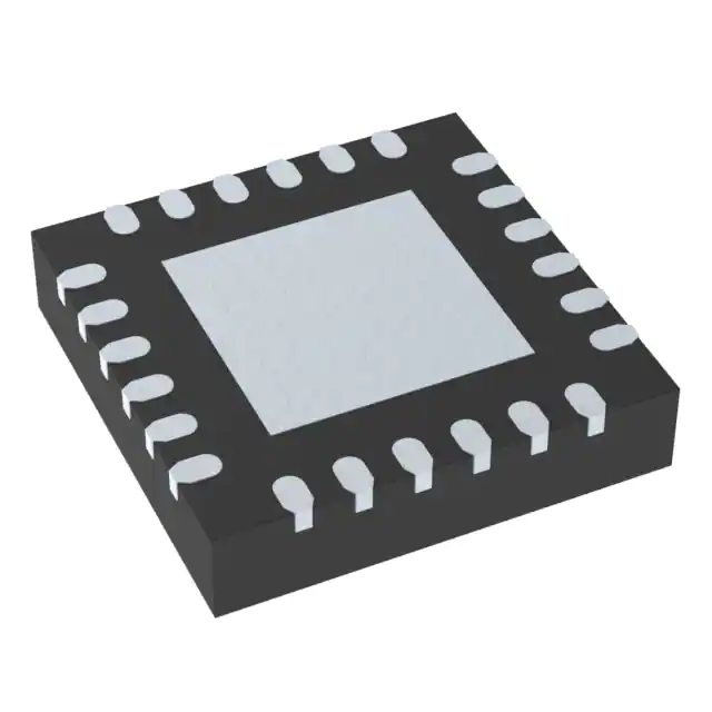
- Part No.:
- SI5338Q-B05073-GMR
- Manufacturer:
- Skyworks Solutions Inc.
- Category:
- Application Specific Clock/Timing
- Package:
- 24-VFQFN Exposed Pad
- Datasheet:
-
 SI5338Q-B05073-GMR.pdf
- Description:
- I2C CONTROL, 4-OUTPUT, ANY FREQU
- Quantity:
- Payment:

- Shipping:

Inventory:3,217
Please send an inquiry. Send us your inquiry, and we will respond immediately.
Product details
Overview
SI5338Q-B05073-GMR from Skyworks Solutions is an I²C-programmable quad clock generator IC with four independently configurable differential or single-ended outputs, 0.7 ps RMS typical phase jitter, PCIe Gen 1–4 Common Clock and Gen 3 SRNS compliance, and operation from 1.8/2.5/3.3 V core supply in a 4 × 4 mm 24-QFN package. It replaces up to four crystal oscillators in Ethernet switch/router and FPGA clocking systems.
For engineers reviewing the SI5338Q-B05073-GMR datasheet, SI5338Q-B05073-GMR pinout, SI5338Q-B05073-GMR application, or SI5338Q-B05073-GMR equivalent, key selection considerations include its MultiSynth™-based any-frequency synthesis (0.16–710 MHz per output), independent output voltage per driver (1.5/1.8/2.5/3.3 V), spread-spectrum capability (0.5–5.0% spread, 33–63 kHz modulation), and loss-of-lock/loss-of-signal alarm support.
Technical Context
The SI5338Q-B05073-GMR implements a two-stage PLL architecture: a high-stability reference stage (with crystal or external clock input) followed by four independent MultiSynth™ fractional-N synthesis paths. Each path supports integer or fractional mode operation, enabling true zero-ppm frequency accuracy across all outputs.
It features fully programmable output drivers supporting LVPECL/LVDS/HCSL/CMOS/SSTL/HSTL formats, independent phase adjustment (<20 ps steps), and glitchless frequency increment/decrement in 1 ppm steps. The device operates over –40 to +85 °C and includes internal OTP NVM for configuration storage.
Key Specifications
| Parameter | Value and Actual Design Meaning |
|---|---|
| Phase Jitter (RMS) | 0.7 ps typical (12 kHz–20 MHz); meets PCIe Gen 3 SRNS & Gen 4 common clock jitter requirements |
| Output Frequency Range | 0.16–710 MHz per channel; supports LVPECL/LVDS up to 710 MHz, HCSL up to 250 MHz, CMOS up to 200 MHz |
| Input Reference Options | Crystal (8–30 MHz), CMOS (5–200 MHz), SSTL/HSTL (5–350 MHz), differential (5–710 MHz) |
| Supply Voltages | Core: 1.8/2.5/3.3 V ±10%; Output buffers: independently configurable 1.5/1.8/2.5/3.3 V |
| Package | 24-pin QFN, 4 × 4 mm, 0.5 mm pitch; RoHS-compliant, moisture sensitivity level 3 |
| Operating Temperature | –40 °C to +85 °C ambient; validated for industrial and telecom line card environments |
| Power Consumption | 45 mA typical core current at 100 MHz on all outputs and 25 MHz reference clock |
Pinout & Package
SI5338Q-B05073-GMR is housed in a 24-lead, 4 × 4 mm QFN package with exposed thermal pad. Pin assignments follow the standard Si5338 top-view layout: IN1/IN2 (differential ref 1), IN3/IN4 (single-ended ref 2), IN5/IN6 (differential ref 3), CLK0A/CLK0B through CLK3A/CLK3B (four differential output pairs), VDDO0–VDDO3 (independent output supply pins), VDD (core supply), SCL/SDA (I²C interface), INTR (interrupt output), and RSVD_GND (reserved ground).
| Pin/Terminal | Circuit Role | Design Meaning |
|---|---|---|
| IN1, IN2 | Differential reference input 1 | Accepts 5–710 MHz AC-coupled differential clock; requires external 100 Ω termination |
| CLK0A, CLK0B | Differential output 0 pair | Configurable format (LVPECL/LVDS/HCSL/CML); driven by MultiSynth₀ with independent voltage (VDDO0) |
| VDDO0 | Output buffer supply 0 | Supplies power to CLK0A/CLK0B driver; selectable 1.5/1.8/2.5/3.3 V for level translation |
| SCL, SDA | I²C serial interface | Standard SMBus-compatible 100/400 kHz interface for configuration and status readback |
| INTR | Interrupt output | Open-drain active-low signal indicating loss of lock, loss of signal, or other fault conditions |
Key Features
| Feature | Design Value |
|---|---|
| Any-frequency synthesis per output | Four independent MultiSynth™ engines enable simultaneous generation of unrelated frequencies (e.g., 100 MHz, 125 MHz, 156.25 MHz, 312.5 MHz) with 0 ppm error |
| PCIe Gen 4 Common Clock compliance | 0.15–0.45 ps RMS jitter (10 kHz–50 MHz) satisfies PCIe Base Spec 4.0 rev 0.5 timing budget for common clock topology |
| Independent output voltage per channel | VDDO0–VDDO3 allow mixed-voltage clock distribution (e.g., 1.8 V LVDS to FPGA, 3.3 V CMOS to microcontroller) without external level shifters |
| Glitchless frequency tuning | Pin-controlled or I²C-based frequency increment/decrement in 1 ppm steps enables real-time clock rate adaptation without output interruption |
| Programmable spread spectrum | Configurable SSC on any output: 0.5–5.0% spread depth, 33–63 kHz modulation rate, reducing EMI peak emissions in dense PCB layouts |
Applications
| Ethernet Switch/Routing System | PCIe Gen 3/4 Add-in Card |
|---|---|
|
Use Scenario: High-density 10 GbE/25 GbE switch fabric requiring synchronized clocks across multiple PHYs, MACs, and packet processors. IC Role / Device Role / Timing Role: Quad clock generator providing four independent low-jitter clocks: 156.25 MHz for SerDes, 100 MHz for CPU interface, 125 MHz for management controller, and 250 MHz for packet buffer memory. Use Value: Eliminates four discrete oscillators and reduces board area by >60%; jitter performance ensures <10⁻¹² BER under worst-case crosstalk and power noise. |
Use Scenario: GPU or NVMe SSD add-in card needing PCIe reference clock plus auxiliary clocks for flash controller and thermal management MCU. IC Role / Device Role / Timing Role: PCIe Gen 3 SRNS-compliant clock source delivering 100 MHz PCIe REFCLK plus 50 MHz for flash interface and 32.768 kHz for RTC, all from single device. Use Value: Meets Intel's PCIe clock jitter spec (0.11–0.32 ps RMS) while enabling spread-spectrum on non-REFCLK outputs to pass FCC Class B emissions testing. |
| Broadcast Video Timing System | FPGA-Based Prototyping Platform |
|
Use Scenario: SMPTE ST 2082 (12G-SDI) video processing system requiring precise 297 MHz pixel clock plus genlock and audio sample clocks. IC Role / Device Role / Timing Role: Any-frequency synthesizer generating 297 MHz (12G-SDI), 27 MHz (genlock), 48 kHz (audio), and 10 MHz (reference) simultaneously with sub-20 ps inter-channel skew. Use Value: Achieves broadcast-grade timing stability (±0.1 ppm) and eliminates manual crystal selection; phase adjustment enables frame-accurate synchronization across multiple video pipelines. |
Use Scenario: Xilinx or Intel FPGA development board requiring flexible clock sources for transceivers, logic fabric, DDR interfaces, and debug peripherals. IC Role / Device Role / Timing Role: Configurable clock hub supplying 148.5 MHz (HDMI TX), 100 MHz (FPGA fabric), 200 MHz (DDR3), and 1 MHz (watchdog timer) - all programmable via I²C during runtime. Use Value: Enables rapid prototyping across multiple IP cores without hardware respins; ClockBuilder Pro GUI simplifies register configuration and validation. |
Equivalent & Alternatives
The following parts are listed as comparable options for similar quad clock generator applications.
| Alternative Part | Technical Difference | Application Difference | Selection Advice |
|---|---|---|---|
| Si5332A-D05089-GM | Higher integration: 8 outputs, integrated crystal, lower jitter (0.35 ps RMS), but larger 32-QFN package and higher cost | Preferred for new designs requiring >4 outputs or crystal-free BOM; not drop-in compatible due to pin count and footprint change | Select when needing more outputs or ultra-low jitter; requires PCB redesign and firmware update for I²C register map differences |
| ICS8430I-01T | Fixed-frequency quad LVDS generator (no I²C programming); 1.2 ps RMS jitter; 3.3 V only; no spread spectrum or phase adjustment | Suitable only for static clock trees where frequencies never change; lacks dynamic tuning and multi-voltage support | Choose only for cost-sensitive, fixed-configuration applications where programmability is unnecessary and jitter margin is sufficient |
Compared with SI5338Q-B05073-GMR, the Si5332A offers superior jitter and integration but demands layout changes, while the ICS8430I sacrifices flexibility for lower unit cost and simpler validation - making SI5338Q-B05073-GMR the optimal balance of programmability, performance, and footprint for mid-volume industrial and networking designs.
Availability
SI5338Q-B05073-GMR is available at Aetrix Electronics and suitable for Ethernet switch/router, PCIe Gen 3/4 add-in cards, and broadcast video timing systems requiring stable component supply, long-term lifecycle support, and guaranteed traceable sourcing.
Supply support for SI5338Q-B05073-GMR includes scheduled delivery planning, volume procurement assistance, BOM continuity management, traceable sourcing, and lifecycle availability coordination for OEM customers, industrial embedded developers, connected-device designers, and electronics production programs.
Manufacturer
Skyworks Solutions is a global leader in analog and mixed-signal semiconductors, specializing in RF, timing, and connectivity solutions for infrastructure, automotive, and mobile markets.
The Si5338 family was designed as a programmable, low-jitter clock generator platform targeting high-speed serial interfaces (PCIe, Ethernet, Fibre Channel) and FPGA/ASIC clocking in space-constrained, thermally demanding applications.
FAQ
What is the primary function of the SI5338Q-B05073-GMR in a timing architecture?
The SI5338Q-B05073-GMR serves as an I²C-programmable quad clock generator that synthesizes four independent, low-jitter output frequencies from a single reference input. Its MultiSynth™ technology enables zero-ppm accuracy across all outputs, replacing multiple discrete oscillators while supporting PCIe Gen 1–4, Ethernet, and broadcast video timing standards. SI5338Q-B05073-GMR integrates PLL-based synthesis, configurable output drivers, and on-chip OTP memory for factory-programmed configurations.
Does the SI5338Q-B05073-GMR support spread-spectrum clocking (SSC), and if so, what are its configurable parameters?
Yes, the SI5338Q-B05073-GMR supports fully programmable spread-spectrum clocking on any output. It allows spread depth from 0.5% to 5.0%, modulation rates from 33 kHz to 63 kHz, and operation across output frequencies from 5 MHz to 350 MHz. These settings are configured via I²C registers and can be enabled/disabled per output independently. SI5338Q-B05073-GMR's SSC implementation helps reduce electromagnetic interference (EMI) peaks in high-density PCB layouts without affecting timing integrity.
Can the SI5338Q-B05073-GMR generate different output voltage levels simultaneously on its four channels?
Yes, the SI5338Q-B05073-GMR supports independent output supply voltages per channel via dedicated VDDO0–VDDO3 pins. Each can be set to 1.5 V, 1.8 V, 2.5 V, or 3.3 V, enabling mixed-signal clock distribution - for example, 1.8 V LVDS to an FPGA transceiver bank and 3.3 V CMOS to a legacy microcontroller - without external level translators. This capability is intrinsic to SI5338Q-B05073-GMR's architecture and requires no additional components.
What reference inputs does the SI5338Q-B05073-GMR accept, and what are their frequency ranges?
The SI5338Q-B05073-GMR accepts six reference inputs: two differential pairs (IN1/IN2, IN5/IN6) supporting 5–710 MHz; two single-ended inputs (IN3, IN4) supporting 5–200 MHz CMOS or 5–350 MHz SSTL/HSTL; and an on-chip oscillator for 8–30 MHz crystals. All references feed into a flexible input multiplexer, allowing dynamic switching between sources. SI5338Q-B05073-GMR's wide input range supports legacy and next-generation timing architectures without external conditioning.
How is the SI5338Q-B05073-GMR programmed, and is external nonvolatile memory required?
The SI5338Q-B05073-GMR is programmed via its I²C/SMBus-compatible serial interface using Skyworks' ClockBuilder Pro software, which auto-generates register maps and validates configurations. It contains on-chip one-time-programmable (OTP) NVM that stores the default configuration, eliminating the need for external EEPROM or Flash. After programming, SI5338Q-B05073-GMR boots with the stored settings and remains functional without host intervention - ideal for unattended systems.
SI5338Q-B05073-GMR Specifications
- Product attributes
- Attribute value
- Manufacturer:
- Skyworks Solutions Inc.
- Series:
- MultiSynth™
- Package/Case:
- 24-VFQFN Exposed Pad
- Packaging:
- Tape & Reel (TR)
- Product Status:
- Active
- Programmable:
- Not Verified
- PLL:
- -
- Main Purpose:
- -
- Input:
- -
- Output:
- -
- Number of Circuits:
- -
- Ratio - Input:Output:
- -
- Differential - Input:Output:
- -
- Frequency - Max:
- -
- Voltage - Supply:
- -
- Operating Temperature:
- -
- Mounting Type:
- Surface Mount
- Grade:
- -
- Qualification:
- -
- Supplier Device Package:
- 24-QFN (4x4)
SI5338Q-B05073-GMR FAQ
1.How can I place an order for SI5338Q-B05073-GMR through Aetrix?
Please submit a Request for Quotation (RFQ) for SI5338Q-B05073-GMR on Aetrix. Our sales agent will provide a competitive quotation and guide you through the order confirmation once you accept the terms.
2.Are the price and stock information for SI5338Q-B05073-GMR reliable?
The price and inventory of SI5338Q-B05073-GMR are updated periodically and may fluctuate due to market conditions. Stock and pricing data are typically refreshed every 24 hours. Quotation validity for SI5338Q-B05073-GMR is usually 5 days.
3.What payment methods are accepted for SI5338Q-B05073-GMR?
We accept Wire Transfer, PayPal, Credit Card, Western Union, MoneyGram, and Escrow for SI5338Q-B05073-GMR transactions.
Note: Certain payment methods may incur a processing fee.
4.How is shipping managed for SI5338Q-B05073-GMR?
SI5338Q-B05073-GMR orders can be shipped via leading logistics carriers, including DHL, UPS, FedEx, TNT, or Registered Mail.
Once your SI5338Q-B05073-GMR order is processed, you will receive an email with the shipment details and tracking number.
Note: Tracking information may take up to 24 hours to appear. Express delivery typically takes 3–5 business days.
5.How can I obtain technical support or documentation for SI5338Q-B05073-GMR?
For technical support, including SI5338Q-B05073-GMR datasheets, pinout diagrams, or application guidance, please contact our engineering support team. They can provide detailed documentation and assistance for your SI5338Q-B05073-GMR requirements.
6.How does Aetrix verify that SI5338Q-B05073-GMR is sourced from the original manufacturer or authorized distributors?
All SI5338Q-B05073-GMR products on Aetrix are procured from qualified distributors and authorized channels. Our dedicated quality assurance team conducts strict verification, including traceability checks and, if necessary, third-party testing. This ensures that SI5338Q-B05073-GMR meets industry standards.
7.What is the process for return or replacement of SI5338Q-B05073-GMR?
All SI5338Q-B05073-GMR units undergo pre-shipment inspection (PSI). If there is an issue with SI5338Q-B05073-GMR, returns or replacements are accepted under the following conditions:
1.Quantity discrepancies, incorrect items, or visible external defects (such as breakage or corrosion), acknowledged by Aetrix.
2.The issue is reported within 90 days of delivery.
3.The SI5338Q-B05073-GMR part is unused and in its original packaging.
Return procedure for SI5338Q-B05073-GMR:
1.Submit a request within 90 days.
2.Obtain a Return Material Authorization (RMA) from Aetrix.
SI5338Q-B05073-GMR Tags
-
LMK00334RTVRQ1
Texas Instruments
.jpg)
-
DSC557-0344FI0T
Microchip Technology
-
9FGV0241AKILFT
Renesas

-
9DBL0452CKILFT
Renesas
-
DSC557-0344FL1T
Microchip Technology
-
RC19008AGND#KB0
Renesas
-
RC19008AGND#BB0
Renesas

-
9DB403DGILFT
Renesas
-
9DB233AGILFT
Renesas

-
9DB803DGILFT
Renesas
-
9FGL0851DKILFT
Renesas
-
AB-557-03-HCHC-F-L-C-T
Abracon LLC
Tech Hub

Counterfeit components can hide behind convincing markings and passing basic function tests. This engineering reference covers source traceability, external inspection, X-ray, XRF, electrical testing, …

A practical engineering and sourcing framework covering lifecycle verification, lifetime-buy calculations, replacement qualification, supplier checks and counterfeit-risk controls.

TTL and CMOS logic families differ in thresholds, loading, output drive, power and timing. This engineering guide compares 74HC and 74HCT, calculates noise margins and checks 3.3 V/5 V compatibility.

A practical engineering guide to 3.3V and 5V logic compatibility, input thresholds, resistor dividers, translator ICs, MOSFET level shifting, I2C pull-ups, timing limits and power-sequencing risks.

The 74HC595 uses push-pull logic outputs, while the TPIC6B595 uses 50 V open-drain DMOS sinks for higher-power loads. This guide compares timing, current limits, 3.3 V interfacing, load wiring, thermal…

The 74HC595 converts serial data into eight stable parallel outputs. This guide covers pin functions, shift and storage timing, OE and MR behavior, drive-current limits, cascading, voltage compatibilit…

A technical comparison of level-sensitive latches and edge-triggered flip-flops, covering timing windows, setup and hold limits, master–slave operation, time borrowing, race-through, HDL inference and…

A D latch stores one bit while Enable controls when data can pass. This reference covers gate-level operation, truth tables, transparency, setup and hold timing, LE versus OE, common ICs and practical …

An SR latch stores one bit through cross-coupled feedback. This engineering reference covers NOR and NAND implementations, truth tables, forbidden-state recovery, gated operation, switch debouncing, fa…

Latch circuits retain one bit through feedback. This technical reference covers SR and D latches, truth tables, transparency, timing limits, latch-versus-flip-flop behavior, applications and common log…


