
 My Inquiry
 My Account


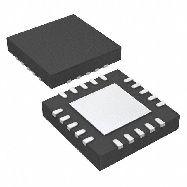
Skyworks Solutions Inc. SI5350A-B06870-GM
- Part No.:
- SI5350A-B06870-GM
- Manufacturer:
- Skyworks Solutions Inc.
- Package:
- 20-VFQFN Exposed Pad
- Datasheet:
-
 SI5350A-B06870-GM.pdf
- Description:
- IC ANY FREQ ANY OUT XTAL 20QFN
- Quantity:
- Payment:

- Shipping:

Inventory:1,747
Please send an inquiry. Send us your inquiry, and we will respond immediately.
Product details
Overview
SI5350A-B06870-GM from Skyworks Solutions is a factory-programmed, pin-controlled CMOS clock generator delivering up to 8 independent output frequencies (2.5 kHz–200 MHz) with 0 ppm synthesis error, low period jitter (<70 ps pk-pk), and configurable spread spectrum on any output. It replaces multiple crystals/XOs in audio/video systems, residential gateways, and networking equipment using a single 25 or 27 MHz crystal reference.
For engineers reviewing the SI5350A-B06870-GM datasheet, SI5350A-B06870-GM pinout, SI5350A-B06870-GM application, or SI5350A-B06870-GM equivalent, key selection considerations include its 20-QFN (4×4 mm) package with 20 pins, dual-PLL + fractional MultiSynth architecture, independent VDD/VDDO voltage scaling (1.8/2.5/3.3 V), and support for glitchless frequency switching via FS_0/FS_1 control pins.
Technical Context
The SI5350A-B06870-GM implements two high-frequency PLLs (PLLA and PLLB) feeding eight independent fractional MultiSynth™ dividers-one per output-enabling simultaneous non-integer-related frequencies. PLLA supports spread spectrum modulation (±0.1% to ±1.5% center-spread or –0.1% to –2.5% down-spread at 31.5 kHz), while PLLB provides low-jitter outputs without spread spectrum.
It accepts only a fixed-frequency crystal (25 or 27 MHz) on XA/XB inputs, with internal load capacitance options (0/6/8/10 pF). Output buffers are individually powered via four VDDO pins (VDDOA–VDDOD), each supporting 1.8/2.5/3.3 V, enabling level translation and HCSL-compatible swing (with external termination) when VDDO = 2.5 V.
Key Specifications
| Parameter | Value and Actual Design Meaning |
|---|---|
| Output count | 8 independent CMOS clock outputs (CLK0–CLK7) |
| Frequency range | 2.5 kHz to 200 MHz per output; max two unique frequencies >112.5 MHz simultaneously |
| Period jitter | <70 ps pk-pk (typical, all outputs active, worst-case frequency plan) |
| Core supply | VDD = 1.8 V / 2.5 V / 3.3 V; supports independent sequencing with VDDO |
| Output supply | Four VDDO rails (VDDOA–VDDOD), each configurable at 1.8/2.5/3.3 V for level translation |
| Reference input | 25 MHz or 27 MHz fundamental-mode AT-cut crystal only (no CLKIN support) |
| Control interface | Pin-strapped configuration (P0–P4); no I²C bus required |
Pinout & Package
SI5350A-B06870-GM is packaged in a 20-pin QFN (4 mm × 4 mm, 0.5 mm pitch) with exposed thermal pad. Pin functions are validated per Skyworks Rev. 1.2 datasheet Section 7.1.
| Pin/Terminal | Circuit Role | Design Meaning |
|---|---|---|
| XA, XB | Crystal oscillator input | Differential crystal connection; supports 25 or 27 MHz AT-cut crystals with internal load capacitance (0/6/8/10 pF) |
| CLK0–CLK7 | CMOS clock outputs | Eight configurable outputs; each driven by dedicated MultiSynth divider; rise/fall time ≤1.5 ns (20–80%, CL = 5 pF) |
| VDDOA–VDDOD | Output buffer supplies | Four independent VDDO rails powering output banks: VDDOA (CLK0/1), VDDOB (CLK2/3), VDDOC (CLK4/5), VDDOD (CLK6/7) |
| VDD | Core supply | 1.8/2.5/3.3 V core power; must be powered before or concurrently with all VDDO rails |
| GND | Ground reference | Eight GND pins (pins 2, 4, 6, 8, 10, 12, 14, 19) ensure low-noise return paths for core and outputs |
| P0–P4 | Configurable control inputs | P0 (FS_0), P1 (FS_1), P2 (SSEN), P3 (PDN), P4 (OEB_2); logic thresholds scale with VDD |
| EPAD | Thermal pad | Exposed copper pad (pin 20) for PCB thermal relief; requires solder connection to ground plane |
Key Features
| Feature | Design Value |
|---|---|
| Factory-programmed frequency plan | Preconfigured at Skyworks for exact SI5350A-B06870-GM output frequencies-no field programming required |
| Glitchless frequency switching | F1_x/F2_x dual-frequency mode on CLK0–CLK2 enabled via FS_0/FS_1 pins; zero-cycle transition between frequencies |
| HCSL-compatible outputs | Configurable with 2.5 V VDDO and external 511 Ω/240 Ω termination to meet HCSL jitter and swing requirements |
| Spread spectrum per-output control | SSEN pin disables spread spectrum globally; individual outputs assigned to PLLA can be modulated independently in ClockBuilder Pro |
| Low-power operation | 25 mA typical core current (8 outputs enabled); 50 µA power-down current with PDN asserted high |
| PSRR robustness | Eliminates need for external LDO filtering due to excellent power supply rejection across VDD and VDDO rails |
Applications
| Audio/Video Processing | Residential Gateway |
|---|---|
Use Scenario: HDMI transmitter, audio codec, and video processor require synchronized clocks at 74.25 MHz, 24.576 MHz, and 48 MHz within a single set-top box. IC Role / Device Role / Timing Role: SI5350A-B06870-GM generates all three frequencies simultaneously from one 27 MHz crystal, replacing discrete oscillators and reducing BOM count. Use Value: Eliminates timing skew between subsystems, enables dynamic frequency switching for power savings, and reduces EMI via per-output spread spectrum. |
Use Scenario: DSL/cable gateway integrates CPU, Ethernet PHY, USB controller, and Wi-Fi SoC-each requiring distinct clock domains (33.33 MHz, 125 MHz, 48 MHz, 28.322 MHz). IC Role / Device Role / Timing Role: SI5350A-B06870-GM serves as central clock source, distributing eight precisely aligned clocks with <70 ps period jitter. Use Value: Enables deterministic latency across interfaces, simplifies layout by removing multiple XO footprints, and supports FCC/CE compliance via programmable spread spectrum. |
| Networking Equipment | XO Replacement |
Use Scenario: Small-form-factor switch uses 10/100/1000BASE-T PHYs requiring 25 MHz, 125 MHz, and 28.322 MHz clocks with tight jitter budgets. IC Role / Device Role / Timing Role: SI5350A-B06870-GM delivers all required frequencies with cycle-to-cycle jitter <150 ps pk-pk (all outputs active), meeting IEEE 802.3 jitter specs. Use Value: Avoids costly low-jitter XOs per interface; allows shared crystal reference across PHYs to improve system-level phase alignment. |
Use Scenario: Legacy design uses four separate 25 MHz XOs for CPU, GPU, memory, and peripheral buses-causing board space and cost pressure. IC Role / Device Role / Timing Role: SI5350A-B06870-GM replaces all four XOs with a single 20-QFN device generating identical 25 MHz clocks on four outputs plus spares. Use Value: Reduces PCB area by >60%, cuts component cost by ~40%, and improves long-term frequency stability via single-crystal reference. |
Equivalent & Alternatives
The following parts are listed as comparable options for similar clock generator applications.
| Alternative Part | Technical Difference | Application Difference | Selection Advice |
|---|---|---|---|
| Si5350A-B06871-GM | Same 20-QFN package and architecture; factory-programmed for different frequency set (e.g., includes 22.5792 MHz and 27 MHz outputs) | Targeted at broadcast video systems requiring SMPTE 259M/292M sync rates | Select only if exact output frequencies match design requirements; not interchangeable without requalification. |
| Si5351A-B-GM | I²C-programmable (not factory-configured); 8 outputs; supports CLKIN (not crystal-only); higher typical jitter (95 ps pk-pk) | Suitable for prototyping or field-upgradable systems where runtime reconfiguration is needed | Choose Si5351A-B-GM only when I²C control and input flexibility outweigh need for guaranteed 0 ppm error and lower jitter of SI5350A-B06870-GM. |
Compared with Si5350A-B06871-GM, SI5350A-B06870-GM offers a fixed, optimized frequency plan for audio/video timing; compared with Si5351A-B-GM, it trades programmability for superior jitter performance, lower EMI, and simpler pin-strapped deployment in volume production.
Availability
SI5350A-B06870-GM is available at Aetrix Electronics and suitable for audio/video processing, residential gateway, and networking equipment requiring stable component supply, long-lifecycle availability, and factory-verified timing accuracy.
Supply support for SI5350A-B06870-GM includes scheduled delivery planning, volume procurement assistance, BOM continuity management, traceable sourcing, and lifecycle availability coordination for OEM customers, industrial embedded developers, connected-device designers, and electronics production programs.
Manufacturer
Skyworks Solutions is a global semiconductor company specializing in analog and mixed-signal connectivity solutions, with leadership in RF, timing, and precision analog products.
The Si5350A family is designed for cost-sensitive, high-volume applications requiring flexible, low-jitter clock generation from a single crystal-targeting consumer electronics, broadband infrastructure, and embedded systems where XO replacement and EMI reduction are critical.
FAQ
What reference clock does SI5350A-B06870-GM require?
SI5350A-B06870-GM requires a 25 MHz or 27 MHz fundamental-mode AT-cut crystal connected to XA/XB pins. It does not accept external clock signals (CLKIN) or overtone crystals. Internal load capacitance options (0/6/8/10 pF) are configurable via ClockBuilder Pro, and external capacitors ≤2 pF may be added for crystals requiring 12 pF load.
Does SI5350A-B06870-GM support I²C configuration?
No. SI5350A-B06870-GM is factory-programmed and pin-strapped only-no I²C interface is present or functional. Configuration is fixed at manufacture using ClockBuilder Pro; runtime reprogramming is not supported. For I²C-configurable alternatives, consider the Si5351A-B-GM.
Can SI5350A-B06870-GM generate frequencies above 112.5 MHz?
Yes, SI5350A-B06870-GM supports frequencies up to 200 MHz, but only two *unique* frequencies above 112.5 MHz may be active simultaneously. For example, 125 MHz on CLK0 and 130 MHz on CLK1 is allowed; adding 150 MHz on CLK2 violates the specification. Duplicate frequencies (e.g., 125 MHz on four outputs) are permitted.
How is spread spectrum enabled on SI5350A-B06870-GM?
Spread spectrum is configured per-output during factory programming and enabled/disabled globally via the SSEN pin (P2). When SSEN is high, spread spectrum operates at preprogrammed deviation (±0.1% to ±1.5% center-spread or –0.1% to –2.5% down-spread) and modulation rate (31.5 kHz). Outputs tied to PLLB cannot use spread spectrum.
What is the thermal performance of SI5350A-B06870-GM in a 4-layer PCB?
On a standard 4-layer board per JESD51-5/7, SI5350A-B06870-GM (20-QFN) has a junction-to-ambient thermal resistance (θJA) of 41 °C/W and junction-to-board (ΨJB) of 16 °C/W. With proper thermal pad soldering to a solid ground plane, it sustains full 8-output operation at 85 °C ambient without derating.
SI5350A-B06870-GM Specifications
- Product attributes
- Attribute value
- Manufacturer:
- Skyworks Solutions Inc.
- Series:
- -
- Package/Case:
- 20-VFQFN Exposed Pad
- Packaging:
- Strip
- Product Status:
- Active
- Programmable:
- Not Verified
- Type:
- -
- PLL:
- -
- Input:
- -
- Output:
- -
- Number of Circuits:
- -
- Ratio - Input:Output:
- -
- Differential - Input:Output:
- -
- Frequency - Max:
- -
- Divider/Multiplier:
- -
- Voltage - Supply:
- -
- Operating Temperature:
- -
- Mounting Type:
- Surface Mount
- Grade:
- -
- Qualification:
- -
- Supplier Device Package:
- 20-QFN (4x4)
SI5350A-B06870-GM FAQ
1.How can I place an order for SI5350A-B06870-GM through Aetrix?
Please submit a Request for Quotation (RFQ) for SI5350A-B06870-GM on Aetrix. Our sales agent will provide a competitive quotation and guide you through the order confirmation once you accept the terms.
2.Are the price and stock information for SI5350A-B06870-GM reliable?
The price and inventory of SI5350A-B06870-GM are updated periodically and may fluctuate due to market conditions. Stock and pricing data are typically refreshed every 24 hours. Quotation validity for SI5350A-B06870-GM is usually 5 days.
3.What payment methods are accepted for SI5350A-B06870-GM?
We accept Wire Transfer, PayPal, Credit Card, Western Union, MoneyGram, and Escrow for SI5350A-B06870-GM transactions.
Note: Certain payment methods may incur a processing fee.
4.How is shipping managed for SI5350A-B06870-GM?
SI5350A-B06870-GM orders can be shipped via leading logistics carriers, including DHL, UPS, FedEx, TNT, or Registered Mail.
Once your SI5350A-B06870-GM order is processed, you will receive an email with the shipment details and tracking number.
Note: Tracking information may take up to 24 hours to appear. Express delivery typically takes 3–5 business days.
5.How can I obtain technical support or documentation for SI5350A-B06870-GM?
For technical support, including SI5350A-B06870-GM datasheets, pinout diagrams, or application guidance, please contact our engineering support team. They can provide detailed documentation and assistance for your SI5350A-B06870-GM requirements.
6.How does Aetrix verify that SI5350A-B06870-GM is sourced from the original manufacturer or authorized distributors?
All SI5350A-B06870-GM products on Aetrix are procured from qualified distributors and authorized channels. Our dedicated quality assurance team conducts strict verification, including traceability checks and, if necessary, third-party testing. This ensures that SI5350A-B06870-GM meets industry standards.
7.What is the process for return or replacement of SI5350A-B06870-GM?
All SI5350A-B06870-GM units undergo pre-shipment inspection (PSI). If there is an issue with SI5350A-B06870-GM, returns or replacements are accepted under the following conditions:
1.Quantity discrepancies, incorrect items, or visible external defects (such as breakage or corrosion), acknowledged by Aetrix.
2.The issue is reported within 90 days of delivery.
3.The SI5350A-B06870-GM part is unused and in its original packaging.
Return procedure for SI5350A-B06870-GM:
1.Submit a request within 90 days.
2.Obtain a Return Material Authorization (RMA) from Aetrix.
SI5350A-B06870-GM Tags

-
CD74HCT4046AM96
Texas Instruments

-
MC14046BDWR2G
onsemi

-
501MILFT
Renesas
-
CD74HC7046AM
Texas Instruments

-
CDCVF2505PWR
Texas Instruments

-
RC19004A100GNL#KB0
Renesas

-
SI5351A-B-GTR
Skyworks Solutions Inc.

-
CY2305SXI-1T
Infineon Technologies
-
570BILFT
Renesas

-
CDCE913PWR
Texas Instruments
-
CY2305SXI-1HT
Infineon Technologies

-
DS1086LU+T
Analog Devices Inc./Maxim Integrated
Tech Hub

Counterfeit components can hide behind convincing markings and passing basic function tests. This engineering reference covers source traceability, external inspection, X-ray, XRF, electrical testing, …

A practical engineering and sourcing framework covering lifecycle verification, lifetime-buy calculations, replacement qualification, supplier checks and counterfeit-risk controls.

TTL and CMOS logic families differ in thresholds, loading, output drive, power and timing. This engineering guide compares 74HC and 74HCT, calculates noise margins and checks 3.3 V/5 V compatibility.

A practical engineering guide to 3.3V and 5V logic compatibility, input thresholds, resistor dividers, translator ICs, MOSFET level shifting, I2C pull-ups, timing limits and power-sequencing risks.

The 74HC595 uses push-pull logic outputs, while the TPIC6B595 uses 50 V open-drain DMOS sinks for higher-power loads. This guide compares timing, current limits, 3.3 V interfacing, load wiring, thermal…

The 74HC595 converts serial data into eight stable parallel outputs. This guide covers pin functions, shift and storage timing, OE and MR behavior, drive-current limits, cascading, voltage compatibilit…

A technical comparison of level-sensitive latches and edge-triggered flip-flops, covering timing windows, setup and hold limits, master–slave operation, time borrowing, race-through, HDL inference and…

A D latch stores one bit while Enable controls when data can pass. This reference covers gate-level operation, truth tables, transparency, setup and hold timing, LE versus OE, common ICs and practical …

An SR latch stores one bit through cross-coupled feedback. This engineering reference covers NOR and NAND implementations, truth tables, forbidden-state recovery, gated operation, switch debouncing, fa…

Latch circuits retain one bit through feedback. This technical reference covers SR and D latches, truth tables, transparency, timing limits, latch-versus-flip-flop behavior, applications and common log…


