
 My Inquiry
 My Account


Skyworks Solutions Inc. SI8271GA-IS
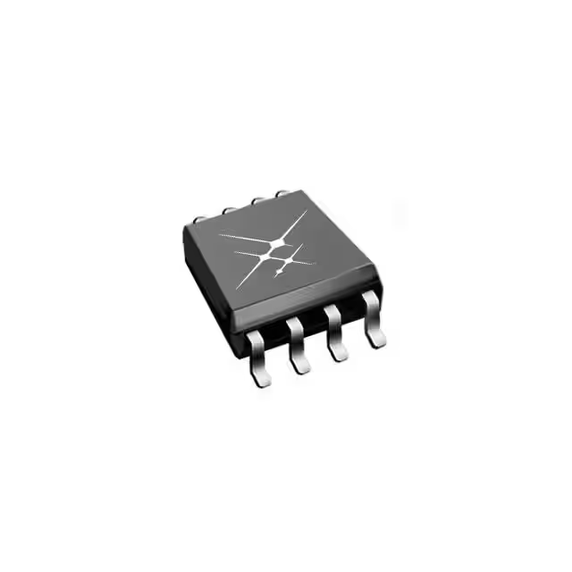
- Part No.:
- SI8271GA-IS
- Manufacturer:
- Skyworks Solutions Inc.
- Category:
- Isolators - Gate Drivers
- Package:
- 8-SOIC (0.154", 3.90mm Width)
- Datasheet:
-
 SI8271GA-IS.pdf
- Description:
- DGTL ISO 1KV 1CH GATE DVR 8SOIC
- Quantity:
- Payment:

- Shipping:

Inventory:1,640
Please send an inquiry. Send us your inquiry, and we will respond immediately.
Product details
Overview
SI8271GA-IS from Skyworks Solutions is a single-channel isolated gate driver IC designed for high-reliability MOSFET/IGBT/SiC/GaN power switch control in isolated half-bridge topologies. It delivers 4 A peak output current, supports 2.5 kVRMS isolation (UL1577), achieves 60 ns max propagation delay, and operates across –40 °C to +125 °C with input supply range 2.5–5.5 V and driver supply 4.2–30 V - enabling use in solar inverters and motor drives requiring robust dV/dt immunity.
For engineers reviewing the SI8271GA-IS datasheet, SI8271GA-IS pinout, SI8271GA-IS application, or SI8271GA-IS equivalent, this page provides verified technical context, exact pin functions, real-world timing and drive capability data, automotive-grade qualification status (AEC-Q100), and validated alternative options for gate driver selection in high-noise power systems.
Technical Context
The SI8271GA-IS implements RF-based silicon isolation with on/off keying modulation across a semiconductor barrier, delivering industry-leading 200 kV/µs common-mode transient immunity (CMTI) and 400 kV/µs latch-up immunity. Its architecture includes independent UVLO monitoring on both input (VDDI) and output (VDD) sides, ensuring safe low-state default during undervoltage conditions.
It features TTL-compatible input with >400 mV hysteresis, dedicated enable (EN) pin for system-level fault shutdown, and separate VO+ / VO– outputs enabling external slew-rate control via discrete pull-up/pull-down networks. No dead-time programming or overlap protection is implemented - consistent with its single-driver, non-PWM, non-HS/LS-pair configuration per Table 4 of the datasheet.
Key Specifications
| Parameter | Value and Actual Design Meaning |
|---|---|
| Isolation Withstand Voltage | 2.5 kVRMS per UL1577 - enables reinforced insulation in 1000 V DC bus systems |
| Peak Output Current | 4.0 A - sufficient to directly drive high-gate-charge SiC FETs (e.g., 100 nC Qg) at 100 kHz with <10 Ω gate resistance |
| Propagation Delay | 60 ns max - supports switching frequencies up to 2 MHz in hard-switched topologies |
| CMTI | 200 kV/µs - maintains signal integrity in fast-switching SiC inverters with >50 V/ns node transients |
| Supply Range | VDDI: 2.5–5.5 V; VDD: 4.2–30 V - allows direct interface with 3.3 V/5 V controllers and flexible gate bias (e.g., 15 V for IGBTs, 12 V for SiC) |
| Operating Temperature | –40 °C to +125 °C - qualified for under-hood automotive and industrial ambient environments |
| Jitter | 200 ps p-p - ensures precise timing alignment in multi-phase interleaved converters |
Pinout & Package
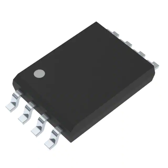
SI8271GA-IS is housed in an 8-pin SOIC package (wide-body, creepage ≥8.0 mm) with gull-wing leads, rated for 2.5 kVRMS isolation and RoHS compliance.
| Pin | Circuit Role | Design Meaning |
|---|---|---|
| 1 (VI) | Digital control input | TTL-compatible logic signal controlling VO+ (high) and VO– (low) states; >400 mV hysteresis prevents noise-induced toggling |
| 2 (VDDI) | Input-side power supply | Supplies isolator transmitter and input logic; must be 2.5–5.5 V; UVLO threshold defined at VDDIUV–/VDDIUV+ |
| 3 (GNDI) | Input-side ground reference | Return path for VI and VDDI; galvanically isolated from driver-side grounds |
| 4 (EN) | Enable control input | Active-high; forces VO+ and VO– low when deasserted; overrides VI state for fail-safe shutdown |
| 5 (GND) | Driver-side ground | Reference for VO– and VDD; must be connected to power stage source/emitter terminal |
| 6 (VO–) | Gate drive pull-low output | Sinks up to 4 A peak; ROL = 1.0 Ω typical - enables fast turn-off with minimal Miller plateau dwell time |
| 7 (VO+) | Gate drive pull-high output | Sources up to 4 A peak; ROH = 2.7 Ω typical - supports strong turn-on even with 15 V gate bias and 5 Ω series resistance |
| 8 (VDD) | Driver-side power supply | Supplies output stage; 4.2–30 V range allows optimization for SiC (12–15 V) or IGBT (15–20 V) gate drive |
Key Features
| Feature | Design Value |
|---|---|
| RF-based silicon isolation | Enables 2.5 kVRMS withstand and 200 kV/µs CMTI without LED aging or temperature drift - 10× longer lifetime vs. optocouplers |
| Separate VO+ / VO– outputs | Allows independent gate resistor placement for asymmetric turn-on/turn-off control - critical for minimizing shoot-through in SiC half-bridges |
| Dedicated EN pin | Provides hardware-level fault response (< tSD) independent of controller firmware - meets ASIL-B functional safety requirements |
| AEC-Q100 qualified | Validated across –40 °C to +125 °C with zero defects in HTOL and TC testing - approved for OBC, traction inverter, and BMS applications |
| UVLO on both sides | Independent monitoring of VDDI and VDD prevents erroneous output states during partial power loss - avoids unintended power device conduction |
Applications
| Solar Power Inverter | Motor Control Drive |
|---|---|
Use Scenario: Isolated gate driving of high-side and low-side SiC MOSFETs in 1500 V DC-link string inverters. IC Role / Device Role / Timing Role: Single SI8271GA-IS per half-bridge leg provides level-shifted, noise-immune control of upper/lower switches with sub-60 ns timing precision. Use Value: 200 kV/µs CMTI prevents false triggering during rapid PV array voltage transients; 4 A drive sustains 100 A phase current with <1 µs switching transitions. |
Use Scenario: Gate driving of IGBT modules in HVAC compressor inverters operating at 16 kHz PWM frequency. IC Role / Device Role / Timing Role: SI8271GA-IS replaces optocoupler-based drivers to eliminate timing skew between parallel legs in 3-phase inverter stacks. Use Value: 200 ps p-p jitter ensures synchronized switching across multiple channels; –40 °C to +125 °C rating supports sealed outdoor enclosure operation. |
| Onboard Charger (OBC) | Uninterruptible Power Supply (UPS) |
Use Scenario: Driving GaN HEMTs in bidirectional AC/DC and DC/DC stages of 11 kW automotive OBCs. IC Role / Device Role / Timing Role: SI8271GA-IS interfaces 3.3 V MCU GPIO to 6 V GaN gate, providing fast, isolated turn-on/turn-off with programmable slew control. Use Value: 60 ns propagation delay enables >500 kHz switching in totem-pole PFC; 4.2–30 V VDD range supports dual-bias schemes (6 V for GaN, 12 V for Si MOSFETs). |
Use Scenario: Controlling IGBTs in double-conversion UPS inverters with 400 V AC output and 600 V DC bus. IC Role / Device Role / Timing Role: SI8271GA-IS serves as isolated gate driver in high-efficiency, transformerless UPS designs requiring reinforced insulation. Use Value: 2.5 kVRMS isolation meets IEC 62109 and UL 1741 requirements; AEC-Q100 qualification ensures field reliability over 10-year service life. |
Equivalent & Alternatives
The following parts are listed as comparable options for similar isolated gate driver applications.
| Alternative Part | Technical Difference | Application Difference | Selection Advice |
|---|---|---|---|
| Si8231AD-IS | Single-channel, 4 A, 5 kVRMS isolation, 35 ns max propagation delay, same 8-pin SOIC package | Lacks EN pin and separate VO+/VO– outputs; uses complementary output pair instead of independent sourcing/sinking | Choose when lower propagation delay is critical and EN functionality or slew control is not required |
| UCC5390SCD | Single-channel, 4 A, 5 kVRMS isolation, integrated Miller clamp, 45 ns max propagation delay, 8-pin SOIC | Includes active Miller clamp and higher CMTI (300 kV/µs); requires external VDD decoupling capacitor | Prefer when driving high-dV/dt SiC devices where Miller-induced turn-on must be actively suppressed |
Compared with SI8271GA-IS, Si8231AD-IS offers faster timing but less system-level fault control, while UCC5390SCD adds Miller clamping at the cost of increased external component count - SI8271GA-IS balances isolation robustness, design flexibility, and automotive qualification in a proven single-driver form factor.
Availability
SI8271GA-IS is available at Aetrix Electronics and suitable for solar power inverters, motor control drives, and onboard chargers requiring stable component supply, long-term lifecycle support, and AEC-Q100-compliant performance.
Supply support for SI8271GA-IS includes scheduled delivery planning, volume procurement assistance, BOM continuity management, traceable sourcing, and lifecycle availability coordination for OEM customers, industrial embedded developers, connected-device designers, and electronics production programs.
Manufacturer
Skyworks Solutions is a global semiconductor company specializing in analog and mixed-signal connectivity solutions, with leadership in RF, timing, and isolation technologies for high-performance wireless and power systems.
The Si827x product line was developed specifically for high-reliability isolated gate driving in EV traction inverters, renewable energy systems, and industrial motor drives - emphasizing CMTI resilience, thermal stability, and automotive qualification from wafer to final test.
FAQ
What is the maximum recommended dV/dt transient the SI8271GA-IS can withstand without malfunction?
The SI8271GA-IS is specified for 200 kV/µs common-mode transient immunity (CMTI) per the datasheet - meaning it reliably maintains correct output state when subjected to voltage transients across its isolation barrier at rates up to 200 kV per microsecond. This value was measured under standard test conditions (IEC 61000-4-4) and applies directly to the SI8271GA-IS. Exceeding this limit may cause temporary output corruption or latch-up, especially in SiC-based 1000 V systems with fast switching edges.
Does the SI8271GA-IS support bootstrap high-side gate driving configurations?
Yes, the SI8271GA-IS supports bootstrap high-side gate driving. Its VO+ and VO– outputs are fully floating relative to GND, allowing VO+ to drive the gate of a high-side N-channel MOSFET or IGBT referenced to a switching node. The datasheet Figure 23A shows a validated half-bridge circuit using SI8273 (same family), and SI8271GA-IS shares identical output architecture and voltage ratings (VDD up to 30 V, VO+ capable of sourcing 4 A into capacitive loads). Bootstrap startup time depends on external capacitor selection and diode forward voltage.
What is the function of the EN pin on the SI8271GA-IS, and how does it interact with UVLO?
The EN pin on the SI8271GA-IS is an active-high enable input that unconditionally forces VO+ and VO– low when pulled low, overriding the VI input state. It operates independently of UVLO - if VDDI falls below UVLO–, EN becomes inactive and outputs remain low regardless of EN state. However, if VDDI is powered but EN is low, the device enters disabled mode within tSD (typ. 100 ns), and resumes normal operation within tRESTART (typ. 300 ns) after EN returns high. This behavior is confirmed in Table 5 and Section 2.5.4 of the SI8271GA-IS datasheet.
Can the SI8271GA-IS drive both SiC MOSFETs and silicon IGBTs effectively?
Yes, the SI8271GA-IS is designed to drive both SiC MOSFETs and silicon IGBTs. Its 4 A peak output current, 2.7 Ω high-side RDS(ON), and 1.0 Ω low-side RDS(ON) support fast switching of devices with gate charges from 20 nC (small SiC) to 300 nC (large IGBTs). The 4.2–30 V VDD range allows optimal bias selection: 12–15 V for SiC, 15–20 V for IGBTs. Datasheet Figures 15–16 confirm rise/fall time and propagation delay performance across load capacitance (1–10 nF) and supply voltage - validating suitability for both technologies.
Is the SI8271GA-IS pin-compatible with other members of the Si827x family such as SI8273 or SI8274?
No, the SI8271GA-IS is not pin-compatible with SI8273 or SI8274. SI8271 uses an 8-pin SOIC package with VI, VDDI, GNDI, EN, GND, VO–, VO+, VDD pinout (Table 1), while SI8273/SI8274 use 16-pin SOIC or LGA-13 packages with dual inputs (VIA/VIB or PWM/DT) and separate VDDA/VDDB supplies. Pin count, function mapping, and supply architecture differ fundamentally - PCB layout and schematic must be redesigned to substitute between these variants. This is explicitly stated in Tables 1–3 and Figure 1 of the datasheet.
SI8271GA-IS Specifications
- Product attributes
- Attribute value
- Manufacturer:
- Skyworks Solutions Inc.
- Series:
- Si827x
- Package/Case:
- 8-SOIC (0.154", 3.90mm Width)
- Packaging:
- Tube
- Product Status:
- Active
- Technology:
- RF Coupling
- Number of Channels:
- 1
- Voltage - Isolation:
- 1000Vrms
- Common Mode Transient Immunity (Min):
- 200kV/µs
- Propagation Delay tpLH / tpHL (Max):
- 75ns, 75ns
- Pulse Width Distortion (Max):
- 8ns
- Rise / Fall Time (Typ):
- 10.5ns, 13.3ns
- Current - Output High, Low:
- 1.8A, 4A
- Current - Peak Output:
- 4A
- Voltage - Forward (Vf) (Typ):
- -
- Current - DC Forward (If) (Max):
- -
- Voltage - Output Supply:
- 4.2V ~ 30V
- Grade:
- -
- Qualification:
- -
- Operating Temperature:
- -40°C ~ 125°C
- Mounting Type:
- Surface Mount
- Supplier Device Package:
- 8-SOIC
- Approval Agency:
- CQC, CSA, UL, VDE
SI8271GA-IS FAQ
1.How can I place an order for SI8271GA-IS through Aetrix?
Please submit a Request for Quotation (RFQ) for SI8271GA-IS on Aetrix. Our sales agent will provide a competitive quotation and guide you through the order confirmation once you accept the terms.
2.Are the price and stock information for SI8271GA-IS reliable?
The price and inventory of SI8271GA-IS are updated periodically and may fluctuate due to market conditions. Stock and pricing data are typically refreshed every 24 hours. Quotation validity for SI8271GA-IS is usually 5 days.
3.What payment methods are accepted for SI8271GA-IS?
We accept Wire Transfer, PayPal, Credit Card, Western Union, MoneyGram, and Escrow for SI8271GA-IS transactions.
Note: Certain payment methods may incur a processing fee.
4.How is shipping managed for SI8271GA-IS?
SI8271GA-IS orders can be shipped via leading logistics carriers, including DHL, UPS, FedEx, TNT, or Registered Mail.
Once your SI8271GA-IS order is processed, you will receive an email with the shipment details and tracking number.
Note: Tracking information may take up to 24 hours to appear. Express delivery typically takes 3–5 business days.
5.How can I obtain technical support or documentation for SI8271GA-IS?
For technical support, including SI8271GA-IS datasheets, pinout diagrams, or application guidance, please contact our engineering support team. They can provide detailed documentation and assistance for your SI8271GA-IS requirements.
6.How does Aetrix verify that SI8271GA-IS is sourced from the original manufacturer or authorized distributors?
All SI8271GA-IS products on Aetrix are procured from qualified distributors and authorized channels. Our dedicated quality assurance team conducts strict verification, including traceability checks and, if necessary, third-party testing. This ensures that SI8271GA-IS meets industry standards.
7.What is the process for return or replacement of SI8271GA-IS?
All SI8271GA-IS units undergo pre-shipment inspection (PSI). If there is an issue with SI8271GA-IS, returns or replacements are accepted under the following conditions:
1.Quantity discrepancies, incorrect items, or visible external defects (such as breakage or corrosion), acknowledged by Aetrix.
2.The issue is reported within 90 days of delivery.
3.The SI8271GA-IS part is unused and in its original packaging.
Return procedure for SI8271GA-IS:
1.Submit a request within 90 days.
2.Obtain a Return Material Authorization (RMA) from Aetrix.
SI8271GA-IS Tags
.JPG)
-
TLP152(TPL,E
Toshiba Semiconductor and Storage

-
HT0740LG-G
Microchip Technology
-
FOD8314TR2
onsemi
-
1EDI60N12AFXUMA1
Infineon Technologies
-
1EDB7275FXUMA1
Infineon Technologies
-
UCC5350MCDR
Texas Instruments

-
2EDB7259KXUMA1
Infineon Technologies

-
UCC5304DWVR
Texas Instruments
-
SI8261BBC-C-ISR
Skyworks Solutions Inc.
-
HT0440LG-G
Microchip Technology
-
HCPL-0302-500E
Broadcom Limited
-
STGAP2HSCMTR
STMicroelectronics
Tech Hub

Counterfeit components can hide behind convincing markings and passing basic function tests. This engineering reference covers source traceability, external inspection, X-ray, XRF, electrical testing, …

A practical engineering and sourcing framework covering lifecycle verification, lifetime-buy calculations, replacement qualification, supplier checks and counterfeit-risk controls.

TTL and CMOS logic families differ in thresholds, loading, output drive, power and timing. This engineering guide compares 74HC and 74HCT, calculates noise margins and checks 3.3 V/5 V compatibility.

A practical engineering guide to 3.3V and 5V logic compatibility, input thresholds, resistor dividers, translator ICs, MOSFET level shifting, I2C pull-ups, timing limits and power-sequencing risks.

The 74HC595 uses push-pull logic outputs, while the TPIC6B595 uses 50 V open-drain DMOS sinks for higher-power loads. This guide compares timing, current limits, 3.3 V interfacing, load wiring, thermal…

The 74HC595 converts serial data into eight stable parallel outputs. This guide covers pin functions, shift and storage timing, OE and MR behavior, drive-current limits, cascading, voltage compatibilit…

A technical comparison of level-sensitive latches and edge-triggered flip-flops, covering timing windows, setup and hold limits, master–slave operation, time borrowing, race-through, HDL inference and…

A D latch stores one bit while Enable controls when data can pass. This reference covers gate-level operation, truth tables, transparency, setup and hold timing, LE versus OE, common ICs and practical …

An SR latch stores one bit through cross-coupled feedback. This engineering reference covers NOR and NAND implementations, truth tables, forbidden-state recovery, gated operation, switch debouncing, fa…

Latch circuits retain one bit through feedback. This technical reference covers SR and D latches, truth tables, transparency, timing limits, latch-versus-flip-flop behavior, applications and common log…


