Send an Inquiry

To receive a quote for your project, please fill in the following information, and we’ll get back to you promptly.

Name*
Company*
Email Address*
Phone/WhatsApp
Part Number*
Quantity*
Message
Submit Inventory List

Please fill in the following information, and we’ll get back to you promptly.

Name*
Company*
Email Address*
Phone/WhatsApp
Upload My List
Message

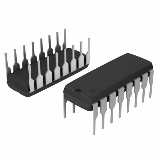
Vishay Siliconix SI9120DJ-E3

Part No.:
SI9120DJ-E3
Manufacturer:
Vishay Siliconix
Category:
AC DC Converters, Offline Switches
Package:
16-DIP (0.300", 7.62mm)
Datasheet:
AetrixSI9120DJ-E3.pdf
Description:
IC OFFLINE SWITCH MULT TOP 16DIP
Quantity:
Payment:
Payment
Shipping:
Shipping

Inventory:4,434

Please send an inquiry. Send us your inquiry, and we will respond immediately.

Part Number
Quantity*
Price
Name*
Company
Email*
Comments

Product details

Overview

SI9120DJ-E3 from Vishay Siliconix is a universal-input, current-mode PWM switchmode controller IC for off-line AC/DC power supplies. It supports 10–450 VDC input, delivers 125 mA peak output drive, integrates a 1 MHz internal oscillator, and operates across −40 °C to +85 °C in a 16-pin PDIP package. It directly drives MOSFETs with Qg ≤ 25 nC in flyback and forward topologies.

For engineers reviewing the SI9120DJ-E3 datasheet, SI9120DJ-E3 pinout, SI9120DJ-E3 application, or SI9120DJ-E3 equivalent, key selection considerations include its high-voltage DMOS input stage, undervoltage lockout (8.1 V), 4 V reference accuracy, 1.2 V current-sense threshold, and compatibility with bootstrap or auxiliary winding bias schemes.

Technical Context

The SI9120DJ-E3 implements current-mode PWM control using a CMOS-based error amplifier and comparator, with a high-voltage BiC/DMOS pre-regulator enabling direct connection to rectified line voltage. Its oscillator frequency (40 kHz–1 MHz) is set externally via ROSC between OSC IN and OSC OUT pins, and the output is duty-cycled to 50% by an internal frequency divider.

SHUTDOWN and RESET inputs operate as latched logic controls with internal pull-up current sources; the latch state determines whether SHUTDOWN is active-high or active-low. The 125 mA push-pull output driver features 20–50 Ω on-resistance and 40–75 ns rise/fall times into 500 pF, supporting direct gate drive of medium-power MOSFETs like IRF820.

Key Specifications

Parameter Value and Actual Design Meaning
Input Voltage Range 10–450 VDC: Enables universal AC input operation without external step-down, suitable for 85–265 VAC mains after bridge rectification.
Oscillator Frequency 40 kHz–1 MHz: Adjustable via external ROSC resistor; 100 kHz typical at ROSC = 330 kΩ - sets switching frequency for EMI and transformer size trade-offs.
Reference Voltage 4.0 V ±2%: Internally trimmed, temperature-compensated zener reference used as error amp non-inverting input - enables precise output voltage regulation.
Current-Sense Threshold 1.2 V (typ): Fixed threshold at SENSE pin - defines overcurrent protection point and peak primary current in current-mode control.
UVLO Threshold 8.1 V (typ): Undervoltage lockout activates below this VCC level - prevents erratic startup and ensures stable gate drive before MOSFET turn-on.
Output Drive Current 125 mA (peak): Sufficient to charge/discharge MOSFET gates with Qg ≤ 25 nC at 100 kHz - eliminates need for external gate driver in ≤30 W designs.
Operating Temperature −40 °C to +85 °C: Industrial-grade thermal range - validated for use in enclosed power adapters and industrial SMPS without derating.

Pinout & Package

SI9120DJ-E3 is housed in a 16-pin plastic dual-in-line package (PDIP), with 0.3 inch body width, 0.1 inch lead pitch, and through-hole mounting. Pins 2 and 3 are not connected (NC). Thermal resistance θJA = 167 °C/W (derated 6 mW/°C above 25 °C).

Pin/Terminal Circuit Role Design Meaning
+VIN (1) High-voltage input supply Connects to rectified DC line; powers internal pre-regulator - requires series resistor for +VIN > 250 V to limit dissipation.
BIAS (16) Bias current reference 390 kΩ to −VIN sets analog section bias current (15 µA nominal) - critical for error amp gain, oscillator stability, and SHUTDOWN/RESET pull-up strength.
FB (4) Error amplifier inverting input Feedback node for output voltage regulation - typically connected to resistive divider from secondary-side optocoupler or auxiliary winding.
COMP (5) Error amplifier output Compensation node for Type II/III loop filter - connects external RC network to stabilize voltage control loop.
SENSE (7) Current-sense input Monitors primary-side current via sense resistor - triggers PWM shutdown when voltage reaches 1.2 V (overcurrent protection).
OUTPUT (8) Gate drive output Push-pull CMOS output driving external MOSFET gate - 125 mA sink/source capability, 20–50 Ω on-resistance, 40–75 ns edge rates.
SHUTDOWN (12) Logic-controlled disable Active-low input with internal 15 µA pull-up - latched or unlatched depending on RESET state per truth table - enables system-level fault response.
−VIN (6) Power ground reference Common return for +VIN, BIAS, and internal high-voltage circuits - must be low-impedance path to minimize noise coupling into analog sections.

Key Features

Feature Design Value
Integrated high-voltage pre-regulator Enables direct +VIN connection up to 450 V without external HV start-up circuit - reduces component count and board space in offline converters.
Current-mode PWM architecture Provides inherent cycle-by-cycle current limiting, improves transient response, and simplifies loop compensation versus voltage-mode control.
Programmable oscillator with external ROSC Allows precise EMI tuning and optimization of transformer size/efficiency trade-offs - no crystal or capacitor required for frequency setting.
Latched SHUTDOWN/RESET logic Prevents unintended restart during fault conditions - ensures safe, controlled shutdown until explicit RESET assertion.
4 V precision reference with high-Z output Supports external override for adaptive regulation schemes while maintaining tight 0.5 mV/°C temperature drift - improves long-term output stability.

Applications

AC/DC Adapters Industrial SMPS

Use Scenario: 12 V/2 A wall adapter for networking equipment operating from 85–265 VAC mains.

IC Role / Device Role / Timing Role: Primary-side PWM controller implementing discontinuous conduction mode (DCM) flyback topology with optocoupler feedback.

Use Value: Eliminates need for external HV start-up circuit and gate driver - reduces BOM cost by ≥3 components while meeting IEC 60950 creepage requirements.

Use Scenario: 24 V/1.5 A DIN-rail mounted power supply for PLC I/O modules in factory automation.

IC Role / Device Role / Timing Role: Current-mode controller in continuous conduction mode (CCM) forward converter with synchronous rectification.

Use Value: 125 mA output drive sustains 100 kHz switching with IRF840 gate charge - achieves >85% efficiency at full load across −25 °C to +70 °C ambient.

LED Driver Supplies Medical Auxiliary Power

Use Scenario: Constant-current LED driver for architectural lighting, accepting universal AC input and delivering 350 mA at 36 V.

IC Role / Device Role / Timing Role: Primary-side controller regulating output current via secondary-side shunt regulator feedback and primary current sensing.

Use Value: 1.2 V SENSE threshold enables accurate current limit setting with <1% tolerance - maintains consistent LED brightness across line and load variations.

Use Scenario: Isolated 5 V/1 A auxiliary supply for patient-monitoring device logic, requiring reinforced insulation and low leakage.

IC Role / Device Role / Timing Role: Flyback controller with transformer-isolated feedback and UVLO ensuring reliable startup only when VCC exceeds 8.1 V.

Use Value: −40 °C to +85 °C rating and 150 °C max junction temperature support extended thermal margin - meets IEC 60601-1 creepage and lifetime requirements.

Equivalent & Alternatives

The following parts are listed as comparable options for similar switchmode controller applications.

Alternative Part Technical Difference Application Difference Selection Advice
UC3842BD1R2G 8-pin SOIC, 16 V max VCC, requires external start-up resistor and gate driver; fixed 250 kHz oscillator. Limited to ≤265 VAC input due to lower +VIN rating; unsuitable for 400 VDC bus applications. Choose UC3842BD1R2G only for cost-sensitive, lower-power (<15 W), non-universal-input designs where layout space is constrained.
NCP1200DR2G 8-pin SOIC, 16 V max VCC, integrated HV start-up but no high-voltage +VIN pin; 65 kHz fixed frequency. Cannot connect directly to rectified line - requires auxiliary winding or external HV supply; lacks programmable oscillator. Select NCP1200DR2G for compact, low-noise 12–24 V input DC/DC controllers where universal AC input is not required.

Compared with UC3842BD1R2G and NCP1200DR2G, the SI9120DJ-E3 uniquely integrates a 450 V-rated +VIN input and programmable oscillator in a single 16-pin package - enabling universal-input flyback designs without external HV circuitry or frequency-setting components.

Availability

SI9120DJ-E3 is available at Aetrix Electronics and suitable for AC/DC adapters, industrial SMPS, LED driver supplies, medical auxiliary power, and DIN-rail power modules requiring stable component supply and long-lifecycle support.

Supply support for SI9120DJ-E3 includes scheduled delivery planning, volume procurement assistance, BOM continuity management, traceable sourcing, and lifecycle availability coordination for OEM customers, industrial embedded developers, connected-device designers, and electronics production programs.

Manufacturer

Vishay Siliconix is a global semiconductor manufacturer specializing in discrete power devices, analog ICs, and passive components, with emphasis on reliability and high-voltage performance.

The SI9120DJ-E3 belongs to Vishay's universal-input switchmode controller product line, designed specifically for compact, high-efficiency offline power conversion in cost-sensitive industrial and consumer applications.

FAQ

What is the maximum input voltage the SI9120DJ-E3 can handle?

The SI9120DJ-E3 supports a +VIN input voltage range of 10 V to 450 V DC. Absolute maximum rating for +VIN is 450 V, and operation above 250 V requires a 10 kΩ, 1/4-W series resistor at Pin 1; above 380 V, a 15 kΩ, 1/4-W resistor is mandatory. This ensures safe pre-regulator operation and avoids exceeding the 5 mA continuous HV input current limit.

Does the SI9120DJ-E3 require an external gate driver?

No, the SI9120DJ-E3 does not require an external gate driver for most applications. Its 125 mA peak output drive and 20–50 Ω on-resistance enable direct drive of MOSFETs with gate charge ≤25 nC - such as IRF820 or BUZ78 - at 100 kHz in ≤30 W flyback or forward converters. Larger MOSFETs increase switching losses but remain feasible with careful layout.

How is the oscillator frequency set on the SI9120DJ-E3?

The oscillator frequency of the SI9120DJ-E3 is set externally using a resistor (ROSC) connected between OSC IN (Pin 9) and OSC OUT (Pin 10). Frequency ranges from 40 kHz to 1 MHz; for example, ROSC = 330 kΩ yields ~100 kHz, and ROSC = 150 kΩ yields ~200 kHz. DISCHARGE (Pin 15) must be tied to −VIN for normal internal oscillator operation.

What is the function of the BIAS pin on the SI9120DJ-E3?

The BIAS pin (Pin 16) on the SI9120DJ-E3 sets the bias current for all analog sections and the internal pull-up current for SHUTDOWN and RESET pins. A 390 kΩ resistor must be connected from BIAS to −VIN (Pin 6) to establish a nominal 15 µA bias current - critical for oscillator stability, error amplifier gain, and proper latch behavior of the control inputs.

Is the SI9120DJ-E3 still in active production?

No, the SI9120DJ-E3 is an end-of-life (EOL) part. Vishay's official documentation states "End of Life. Last Available Purchase Date is 31-Dec-2014." However, Aetrix Electronics maintains legacy inventory and offers traceable, tested units for design continuity, repair, and long-lifecycle industrial programs requiring exact form-fit-function replacement.

SI9120DJ-E3 Specifications

Product attributes
Attribute value
Manufacturer:
Vishay Siliconix
Series:
-
Package/Case:
16-DIP (0.300", 7.62mm)
Packaging:
Bulk
Product Status:
Obsolete
Output Isolation:
Isolated
Internal Switch(s):
No
Voltage - Breakdown:
-
Topology:
Flyback, Forward
Voltage - Start Up:
-
Voltage - Supply (Vcc/Vdd):
9.5V ~ 13.5V
Duty Cycle:
50%
Frequency - Switching:
40kHz ~ 1MHz
Power (Watts):
-
Fault Protection:
-
Control Features:
-
Operating Temperature:
-40°C ~ 85°C (TA)
Grade:
-
Qualification:
-
Supplier Device Package:
16-PDIP
Mounting Type:
Through Hole

SI9120DJ-E3 FAQ

1.How can I place an order for SI9120DJ-E3 through Aetrix?

Please submit a Request for Quotation (RFQ) for SI9120DJ-E3 on Aetrix. Our sales agent will provide a competitive quotation and guide you through the order confirmation once you accept the terms.

2.Are the price and stock information for SI9120DJ-E3 reliable?

The price and inventory of SI9120DJ-E3 are updated periodically and may fluctuate due to market conditions. Stock and pricing data are typically refreshed every 24 hours. Quotation validity for SI9120DJ-E3 is usually 5 days.

3.What payment methods are accepted for SI9120DJ-E3?

We accept Wire Transfer, PayPal, Credit Card, Western Union, MoneyGram, and Escrow for SI9120DJ-E3 transactions.

Note: Certain payment methods may incur a processing fee.

4.How is shipping managed for SI9120DJ-E3?

SI9120DJ-E3 orders can be shipped via leading logistics carriers, including DHL, UPS, FedEx, TNT, or Registered Mail.

Once your SI9120DJ-E3 order is processed, you will receive an email with the shipment details and tracking number.

Note: Tracking information may take up to 24 hours to appear. Express delivery typically takes 3–5 business days.

5.How can I obtain technical support or documentation for SI9120DJ-E3?

For technical support, including SI9120DJ-E3 datasheets, pinout diagrams, or application guidance, please contact our engineering support team. They can provide detailed documentation and assistance for your SI9120DJ-E3 requirements.

6.How does Aetrix verify that SI9120DJ-E3 is sourced from the original manufacturer or authorized distributors?

All SI9120DJ-E3 products on Aetrix are procured from qualified distributors and authorized channels. Our dedicated quality assurance team conducts strict verification, including traceability checks and, if necessary, third-party testing. This ensures that SI9120DJ-E3 meets industry standards.

7.What is the process for return or replacement of SI9120DJ-E3?

All SI9120DJ-E3 units undergo pre-shipment inspection (PSI). If there is an issue with SI9120DJ-E3, returns or replacements are accepted under the following conditions:

1.Quantity discrepancies, incorrect items, or visible external defects (such as breakage or corrosion), acknowledged by Aetrix.

2.The issue is reported within 90 days of delivery.

3.The SI9120DJ-E3 part is unused and in its original packaging.

Return procedure for SI9120DJ-E3:

1.Submit a request within 90 days.

2.Obtain a Return Material Authorization (RMA) from Aetrix.

SI9120DJ-E3 Tags
  • SI9120DJ-E3
  • SI9120DJ-E3 PDF
  • SI9120DJ-E3 Datasheet
  • SI9120DJ-E3 Specifications
  • SI9120DJ-E3 Images
  • Vishay Siliconix
  • Vishay Siliconix SI9120DJ-E3
  • Buy SI9120DJ-E3
  • SI9120DJ-E3 Price
  • SI9120DJ-E3 Distributor
  • SI9120DJ-E3 Supplier
  • SI9120DJ-E3 Wholesale
Related Products
LNK6407D-TL
LNK6407D-TL

Power Integrations

LNK3204D-TL
LNK3204D-TL

Power Integrations

SR10LG-G
SR10LG-G

Microchip Technology

TNY285DG-TL
TNY285DG-TL

Power Integrations

LNK304DN-TL
LNK304DN-TL

Power Integrations

TNY285KG-TL
TNY285KG-TL

Power Integrations

LNK3206D-TL
LNK3206D-TL

Power Integrations

LNK623DG-TL
LNK623DG-TL

Power Integrations

TNY286PG
TNY286PG

Power Integrations

LNK624DG-TL
LNK624DG-TL

Power Integrations

LNK604DG-TL
LNK604DG-TL

Power Integrations

UCC28704DBVR-1
UCC28704DBVR-1

Texas Instruments

Tech Hub

Search

Search

PRODUCT

PRODUCT

PHONE

PHONE

USER

USER