
 My Inquiry
 My Account


NXP Semiconductors SJA1105PELY
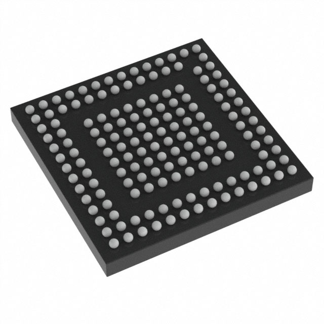
- Part No.:
- SJA1105PELY
- Manufacturer:
- NXP Semiconductors
- Category:
- Controllers
- Package:
- 159-LFBGA
- Datasheet:
-
 SJA1105PELY.pdf
- Description:
- IC ETHERNET SWITCH SPI 159LFBGA
- Quantity:
- Payment:

- Shipping:

Inventory:888
Please send an inquiry. Send us your inquiry, and we will respond immediately.
Product details
Overview
SJA1105PELY from NXP Semiconductors is a 5-port automotive Ethernet switch IC supporting IEEE 802.1Q VLANs, IEEE 802.1AS timestamping, and IEEE 802.1Qav AVB traffic shaping. It operates across 10/100/1000 Mbit/s per port via RGMII/SGMII, features independent 1.8/2.5/3.3 V I/O domains, 1.2 V core voltage, and is qualified to AEC-Q100 Grade 2 (−40 °C to +105 °C) for in-vehicle networking.
For engineers reviewing the SJA1105PELY datasheet, SJA1105PELY pinout, SJA1105PELY application, or SJA1105PELY equivalent, key selection criteria include deterministic AVB timing support, hardware-accelerated credit-based shapers (16 total), IEEE 1588v2 one-step sync forwarding, and LFBGA159 package compatibility with SJA1105T-series cascading designs.
Technical Context
The SJA1105PELY implements a store-and-forward switching architecture with per-port MII/RMII/RGMII/SGMII interface configurability and programmable drive strength. Its hardware timestamping engine complies with IEEE 802.1AS, enabling sub-microsecond synchronization accuracy in time-sensitive networks.
It integrates 16 independently allocatable credit-based shapers per priority queue per port per IEEE 802.1Qav, supports SR Class A/B/C traffic, and delivers IEEE 1588v2 one-step sync forwarding without host CPU intervention - critical for deterministic audio/video bridging in automotive ECUs.
Key Specifications
| Parameter | Value and Actual Design Meaning |
|---|---|
| Port count | 5-port switch with full-duplex operation and per-port speed negotiation (10/100/1000 Mbit/s) |
| VLAN support | 4096 IEEE 802.1Q VLANs with tag insertion/stripping and filtering |
| AVB compliance | Hardware-accelerated IEEE 802.1Qav credit-based shapers (16 total), SR Class A/B/C support |
| Timing precision | IEEE 802.1AS hardware timestamping and IEEE 1588v2 one-step sync forwarding |
| Operating temp | AEC-Q100 Grade 2: −40 °C to +105 °C ambient, qualified for automotive under-hood use |
| I/O voltage | Selectable 1.8 V / 2.5 V / 3.3 V for MII/RMII/RGMII and host interfaces; 1.2 V core |
| Package | LFBGA159 (12 mm × 12 mm), pin-compatible with SJA1105T series |
Pinout & Package
LFBGA159 (12 mm × 12 mm, 0.8 mm pitch) package with 159 solder balls. Ball map follows JEDEC MO-275AC standard for fine-pitch BGA; thermal pad exposed on underside for PCB-level heat dissipation.
| Pin/Terminal | Circuit Role | Design Meaning |
|---|---|---|
| VDDIO_1–VDDIO_5 | I/O supply domain | Independent 1.8/2.5/3.3 V supplies per port group - enables mixed-voltage PHY interfacing |
| VDDCORE | Core power rail | 1.2 V regulated supply required; decoupling critical for AVB timing stability |
| REFCLK_IN | System clock input | 25 MHz single-ended crystal or AC-coupled clock; drives internal PLL for all timing domains |
| SYNC_OUT | Cascading synchronization | Drives REFCLK_IN of downstream SJA1105 devices for multi-chip time alignment |
| SPI_CS/SPI_SCLK/SPI_MOSI/SPI_MISO | Host configuration interface | 4-wire SPI (mode 0, CPOL=0, CPHA=0) for runtime register access and table programming |
Key Features
| Feature | Design Value |
|---|---|
| Per-port interface flexibility | Each port configurable as MII/RMII (10/100), RGMII (10/100/1000), or SGMII - no external level shifters needed |
| Hardware AVB acceleration | 16 credit-based shapers allocated freely across ports and priority queues - eliminates software scheduling latency |
| Deterministic timestamping | IEEE 802.1AS-compliant hardware timestamping at ingress/egress with <100 ns resolution |
| Automotive qualification | AEC-Q100 Rev-H qualified, Grade 2 temperature range - validated for ECU deployment without derating |
| Cascading capability | Synchronization output (SYNC_OUT) and reference clock output (REFCLK_OUT) enable precise multi-switch timing alignment |
Applications
| In-Vehicle Infotainment Backbone | ADAS Sensor Aggregation Hub |
|---|---|
Use Scenario: High-bandwidth video/audio streaming between head unit, displays, and microphones in premium vehicles. IC Role / Device Role / Timing Role: Central AVB-aware Ethernet switch managing synchronized Class A/B traffic with sub-200 µs end-to-end latency. Use Value: Hardware timestamping and credit-based shaping ensure jitter-free audio playback and lip-sync accuracy across distributed ECUs. | Use Scenario: Consolidating camera, radar, and ultrasonic sensor data into central domain controller via time-synchronized Ethernet. IC Role / Device Role / Timing Role: Deterministic switch providing IEEE 1588v2 one-step sync forwarding for sensor timestamp correlation. Use Value: Enables precise sensor fusion by aligning timestamps across heterogeneous sensors without host CPU overhead. |
| Body Control Module Network | Gateway ECU Interconnect |
Use Scenario: Replacing legacy CAN/LIN with Ethernet for lighting, HVAC, and door control modules requiring coordinated actuation. IC Role / Device Role / Timing Role: VLAN-segmented switch isolating safety-critical and non-critical traffic while enforcing QoS policies. Use Value: 4096 VLANs and priority-based QoS allow secure, low-latency control messaging alongside diagnostics and firmware updates. | Use Scenario: Bridging high-speed Ethernet domains (e.g., infotainment, ADAS) with legacy vehicle networks (CAN FD, LIN). IC Role / Device Role / Timing Role: High-throughput switch acting as Ethernet backbone node with hardware-assisted packet filtering and statistics collection. Use Value: Frame drop monitoring and buffer load reporting enable real-time network health assessment for OTA update reliability. |
Equivalent & Alternatives
The following parts are listed as comparable options for similar automotive Ethernet switching applications.
| Alternative Part | Technical Difference | Application Difference | Selection Advice |
|---|---|---|---|
| MARVELL 88Q5050 | Supports TSN (IEEE 802.1Qbv/Qbu/Qci); higher port count (8-port); requires external PHY for 1000BASE-T | Targeted at next-gen zonal architectures needing time-triggered scheduling and security features | Choose when TSN determinism beyond AVB is required; verify PHY interface compatibility and layout complexity |
| TI DP83869HM | Single-port Gigabit Ethernet PHY with integrated RGMII/MII; no switch fabric or VLAN/AVB support | Used as endpoint PHY only - not a functional replacement for switching or AVB functions | Consider only as companion PHY for SJA1105PELY; not a standalone switch alternative |
Compared with MARVELL 88Q5050 and TI DP83869HM, the SJA1105PELY uniquely delivers production-ready AVB switching in an AEC-Q100-qualified 5-port LFBGA159 package with integrated hardware timestamping and credit-based shaping - making it optimal for cost-constrained, volume automotive deployments where full TSN is not yet mandated.
Availability
SJA1105PELY is available at Aetrix Electronics and suitable for in-vehicle infotainment, ADAS sensor aggregation, and body control module applications requiring stable component supply, automotive-grade lifecycle assurance, and AEC-Q100-compliant sourcing.
Supply support for SJA1105PELY includes scheduled delivery planning, volume procurement assistance, BOM continuity management, traceable sourcing, and lifecycle availability coordination for OEM customers, industrial embedded developers, connected-device designers, and electronics production programs.
Manufacturer
NXP Semiconductors is a global semiconductor company specializing in secure connectivity solutions for automotive, industrial, and IoT markets, with leadership in automotive Ethernet and secure MCU technologies.
The SJA1105PELY belongs to NXP's SJA1105P/Q/R/S family - designed specifically for deterministic, low-latency Ethernet switching in automotive ECUs, with native support for AVB, VLAN segmentation, and AEC-Q100 qualification.
FAQ
What is the primary function of the SJA1105PELY in automotive networks?
The SJA1105PELY serves as a 5-port automotive Ethernet switch IC that enables deterministic, time-synchronized communication using IEEE 802.1Qav AVB and IEEE 802.1AS timestamping. It routes traffic between ECUs while enforcing QoS, VLAN isolation, and hardware-accelerated traffic shaping - essential for infotainment, ADAS, and body control systems. The SJA1105PELY integrates all required switching logic without external memory or FPGA assistance.
Does the SJA1105PELY support Gigabit Ethernet speeds on all ports?
Yes, the SJA1105PELY supports 10/100/1000 Mbit/s per port when configured in RGMII or SGMII mode. In MII/RMII mode, it operates at 10/100 Mbit/s. Each port is independently configurable, allowing mixed-speed topologies. The SJA1105PELY achieves full Gigabit throughput with internal delay compensation in RGMII mode - eliminating need for external delay components.
How does the SJA1105PELY achieve IEEE 1588v2 synchronization?
The SJA1105PELY implements IEEE 1588v2 one-step sync forwarding in hardware, embedding precise timestamps directly into PTP sync messages at the egress port. This avoids software-induced jitter and ensures sub-microsecond timestamp accuracy across the network. The SJA1105PELY uses its internal 25 MHz reference clock and hardware timestamping engine to maintain synchronization without host CPU involvement.
Is the SJA1105PELY pin-compatible with other members of the SJA1105 family?
Yes, the SJA1105PELY is pin-compatible with SJA1105TEL and shares the same LFBGA159 package footprint and ball map as specified in the SJA1105P/Q/R/S short data sheet. This allows direct substitution in existing layouts designed for SJA1105T variants, provided configuration tables and firmware are updated to match SJA1105PELY's feature set and register mapping.
What voltage domains does the SJA1105PELY support for I/O interfacing?
The SJA1105PELY supports selectable I/O voltages of 1.8 V, 2.5 V, or 3.3 V for MII/RMII/RGMII interfaces and host processor connections - enabling interoperability with diverse PHYs and SoCs. Its core logic operates at a fixed 1.2 V, requiring dedicated regulation. The SJA1105PELY maintains independent voltage domains per port group to prevent cross-talk and simplify mixed-voltage board design.
SJA1105PELY Specifications
- Product attributes
- Attribute value
- Manufacturer:
- NXP Semiconductors
- Package/Case:
- 159-LFBGA
- Programmable:
- Not Verified
- Protocol:
- Ethernet
- Function:
- Switch
- Interface:
- SPI
- Standards:
- IEEE 802.3
- Voltage - Supply:
- 1.65V ~ 3.6V
- Current - Supply:
- 3.5mA
- Operating Temperature:
- -40°C ~ 125°C (TJ)
- Supplier Device Package:
- 159-LFBGA (12x12)
- Grade:
- Automotive
- Qualification:
- AEC-Q100
SJA1105PELY FAQ
1.How can I place an order for SJA1105PELY through Aetrix?
Please submit a Request for Quotation (RFQ) for SJA1105PELY on Aetrix. Our sales agent will provide a competitive quotation and guide you through the order confirmation once you accept the terms.
2.Are the price and stock information for SJA1105PELY reliable?
The price and inventory of SJA1105PELY are updated periodically and may fluctuate due to market conditions. Stock and pricing data are typically refreshed every 24 hours. Quotation validity for SJA1105PELY is usually 5 days.
3.What payment methods are accepted for SJA1105PELY?
We accept Wire Transfer, PayPal, Credit Card, Western Union, MoneyGram, and Escrow for SJA1105PELY transactions.
Note: Certain payment methods may incur a processing fee.
4.How is shipping managed for SJA1105PELY?
SJA1105PELY orders can be shipped via leading logistics carriers, including DHL, UPS, FedEx, TNT, or Registered Mail.
Once your SJA1105PELY order is processed, you will receive an email with the shipment details and tracking number.
Note: Tracking information may take up to 24 hours to appear. Express delivery typically takes 3–5 business days.
5.How can I obtain technical support or documentation for SJA1105PELY?
For technical support, including SJA1105PELY datasheets, pinout diagrams, or application guidance, please contact our engineering support team. They can provide detailed documentation and assistance for your SJA1105PELY requirements.
6.How does Aetrix verify that SJA1105PELY is sourced from the original manufacturer or authorized distributors?
All SJA1105PELY products on Aetrix are procured from qualified distributors and authorized channels. Our dedicated quality assurance team conducts strict verification, including traceability checks and, if necessary, third-party testing. This ensures that SJA1105PELY meets industry standards.
7.What is the process for return or replacement of SJA1105PELY?
All SJA1105PELY units undergo pre-shipment inspection (PSI). If there is an issue with SJA1105PELY, returns or replacements are accepted under the following conditions:
1.Quantity discrepancies, incorrect items, or visible external defects (such as breakage or corrosion), acknowledged by Aetrix.
2.The issue is reported within 90 days of delivery.
3.The SJA1105PELY part is unused and in its original packaging.
Return procedure for SJA1105PELY:
1.Submit a request within 90 days.
2.Obtain a Return Material Authorization (RMA) from Aetrix.
SJA1105PELY Tags

-
PTN5150AHXMP
NXP Semiconductors

-
USB3740B-AI9-TR
Microchip Technology

-
USB3740B-AI2-TR
Microchip Technology

-
USB3300-EZK-TR
Microchip Technology
-
USB3300-EZK
Microchip Technology

-
FUSB340TMX
onsemi

-
FUSB302BMPX
onsemi

-
DP83826IRHBR
Texas Instruments

-
MCP2518FDT-E/QBB
Microchip Technology
-
FUSB302MPX
onsemi

-
MCP2518FDT-E/SL
Microchip Technology

-
FT260Q-R
FTDI, Future Technology Devices International Ltd
Tech Hub

A practical engineering guide to 3.3V and 5V logic compatibility, input thresholds, resistor dividers, translator ICs, MOSFET level shifting, I2C pull-ups, timing limits and power-sequencing risks.

The 74HC595 uses push-pull logic outputs, while the TPIC6B595 uses 50 V open-drain DMOS sinks for higher-power loads. This guide compares timing, current limits, 3.3 V interfacing, load wiring, thermal…

The 74HC595 converts serial data into eight stable parallel outputs. This guide covers pin functions, shift and storage timing, OE and MR behavior, drive-current limits, cascading, voltage compatibilit…

A technical comparison of level-sensitive latches and edge-triggered flip-flops, covering timing windows, setup and hold limits, master–slave operation, time borrowing, race-through, HDL inference and…

A D latch stores one bit while Enable controls when data can pass. This reference covers gate-level operation, truth tables, transparency, setup and hold timing, LE versus OE, common ICs and practical …

An SR latch stores one bit through cross-coupled feedback. This engineering reference covers NOR and NAND implementations, truth tables, forbidden-state recovery, gated operation, switch debouncing, fa…

Latch circuits retain one bit through feedback. This technical reference covers SR and D latches, truth tables, transparency, timing limits, latch-versus-flip-flop behavior, applications and common log…

An engineering guide to LED driver operation, constant-current and constant-voltage outputs, linear and switching topologies, dimming, IC selection, calculations, replacement compatibility, and fault c…

Operational amplifier guide covering op amp basics, feedback, ideal vs real op amps, common configurations, buffer circuits, offset, bias current, gain-bandwidth, slew rate, rail-to-rail limits and sel…

Jumper cables guide covering safe connection order, red and black clamp placement, final ground connection, cable gauge, length, clamp quality, copper vs CCA cables, jump starter comparison and battery…


