
 My Inquiry
 My Account


Skyworks Solutions Inc. SKY13388-465LF
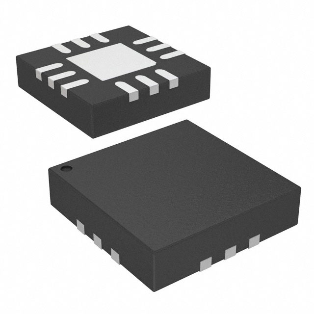
- Part No.:
- SKY13388-465LF
- Manufacturer:
- Skyworks Solutions Inc.
- Category:
- RF Switches
- Package:
- 12-UFQFN Exposed Pad
- Datasheet:
-
 SKY13388-465LF.pdf
- Description:
- IC RF SWITCH SP4T 2.7GHZ 12QFN
- Quantity:
- Payment:

- Shipping:

Inventory:2,170
Please send an inquiry. Send us your inquiry, and we will respond immediately.
Product details
Overview
SKY13388-465LF from Skyworks Solutions is a symmetrical single-pole, four-throw (SP4T) RF switch with integrated logic decoder, designed for broadband antenna switching in WCDMA/CDMA/LTE front-end modules. It operates from 0.05 to 2.7 GHz, delivers 0.60 dB typical insertion loss at 2.2 GHz, >30 dB isolation at 1.0 GHz, and supports 2.5–5.5 V supply with 1.8 V logic compatibility.
For engineers reviewing the SKY13388-465LF datasheet, SKY13388-465LF pinout, SKY13388-465LF application, or SKY13388-465LF equivalent, key selection considerations include its SOI-based high-linearity architecture, QFN-12 (2 × 2 mm) package, integrated 2-bit decoder eliminating external logic, and suitability for diversity receive and multi-band transmit antenna routing in space-constrained mobile RF front-ends.
Technical Context
The SKY13388-465LF implements a silicon-on-insulator (SOI) process enabling high linearity (IIP3 = +65 dBm @ 0.9 GHz) and low distortion (harmonics >75 dBc @ 2.2 GHz), while supporting fast switching (tON/tOFF ≤ 1000 ns) and ultra-low control current (ICTL = 5 μA). Its on-chip energy management uses only two DC control lines (V1/V2) plus EN to select among four RF inputs (RF1–RF4) routed to the common ANT port.
State control follows a defined truth table with explicit shutdown mode (EN = 0), and all unused RF ports are internally terminated when not selected. The device maintains stable RF performance across –40 °C to +85 °C operating temperature and requires no external matching components due to 50 Ω port impedance and >20 dB return loss across full band.
Key Specifications
| Parameter | Value and Actual Design Meaning |
|---|---|
| Frequency Range | 0.05–2.7 GHz: Covers all 3GPP LTE Bands I–XL, WCDMA B1/B2/B5/B8, and CDMA cellular bands without re-tuning. |
| Insertion Loss | 0.60 dB typical @ 2.2 GHz: Minimizes signal attenuation in main path, preserving receiver sensitivity and transmit EVM. |
| Isolation | >30 dB typical @ 1.0 GHz: Prevents crosstalk between active and inactive antenna paths, critical for TDD/FDD coexistence. |
| IIP3 | +65 dBm typical @ 0.9 GHz: Enables high dynamic range operation in crowded spectral environments with strong interferers. |
| Supply Voltage | 2.5–5.5 V: Compatible with standard mobile baseband and PMIC rails; supports battery voltage sag during peak transmit bursts. |
| Logic Compatibility | VHIGH = 1.65–3.3 V, VLOW = 0–0.4 V: Direct interface with 1.8 V GPIOs without level-shifting circuitry. |
| Package | QFN-12, 2 × 2 mm, MSL1: Enables high-density RF layout; exposed pad ensures thermal stability under continuous RF power. |
Pinout & Package
SKY13388-465LF is housed in a 12-pin Quad Flat No-Lead (QFN) package measuring 2.0 × 2.0 × 0.55 mm with an exposed thermal pad (pin 12 must be grounded). The package is moisture sensitivity level 1 (MSL1) rated for 260 °C reflow and compatible with both leaded and lead-free soldering processes.
| Pin/Terminal | Circuit Role | Design Meaning |
|---|---|---|
| 1 (RF1) | RF input port 1 | Primary antenna path for Band 1 or primary diversity receive; 50 Ω matched, no external tuning required. |
| 2 (RF2) | RF input port 2 | Secondary antenna path for Band 3 or secondary diversity branch; identical RF performance to RF1–RF4. |
| 3 (VDD) | DC power supply | Single-supply rail powering internal SOI FETs and decoder; decoupling capacitor required near pin. |
| 4 (EN) | Enable control | Global enable/disable: EN = 0 places device in low-current shutdown state; EN = 1 activates logic decoding. |
| 5 (V1) | Control input bit 1 | LSB of 2-bit address selecting RF1–RF4; driven by baseband processor GPIO with 1.8 V logic levels. |
| 6 (V2) | Control input bit 2 | MSB of 2-bit address; combined with V1 and EN, determines which RF port connects to ANT per Table 4. |
| 7,10,12 (GND) | Ground terminals | Three dedicated ground pins plus exposed pad ensure low-inductance RF return path and thermal dissipation. |
| 8 (RF3) | RF input port 3 | Third antenna path for Band 7 or auxiliary LTE MIMO branch; symmetric insertion loss and isolation. |
| 9 (RF4) | RF input port 4 | Fourth antenna path for Band 40/41 or GPS/Wi-Fi coexistence; supports same frequency range and linearity. |
| 11 (ANT) | RF common antenna port | Single-ended 50 Ω output connected to main antenna feed; handles up to +37 dBm absolute max input power. |
Key Features
| Feature | Design Value |
|---|---|
| Integrated 2-bit logic decoder | Eliminates need for external gate logic or microcontroller GPIO expansion, reducing BOM count and PCB area. |
| Symmetrical SP4T architecture | Equal insertion loss, isolation, and return loss across all four RF paths enables flexible antenna mapping without calibration. |
| SOI process technology | Delivers high linearity (P0.1dB = +36 dBm) and low harmonic distortion (>75 dBc) essential for LTE-A carrier aggregation. |
| No external matching components | All ports internally matched to 50 Ω; simplifies layout, improves yield, and avoids sensitivity to PCB parasitics. |
| Low standby current | ICC = 50 μA @ VDD = 2.6 V enables extended battery life in always-on diversity receive applications. |
Applications
| WCDMA/LTE Front-End Switching | Diversity Receive Antenna Routing |
|---|---|
|
Use Scenario: Dual-antenna LTE smartphone supporting simultaneous transmission on Band 1 and reception on Band 3. IC Role / Device Role / Timing Role: SP4T switch routes transmit signal from PA to primary antenna (RF1→ANT) while connecting secondary antenna (RF2→ANT) to LNA for concurrent diversity receive. Use Value: Enables concurrent Tx/Rx operation without duplexer insertion loss; maintains >30 dB isolation between paths to prevent desensitization. |
Use Scenario: Tablet with four LTE antennas using two for primary diversity and two for secondary diversity in high-mobility environments. IC Role / Device Role / Timing Role: SKY13388-465LF dynamically selects best-performing antenna pair (e.g., RF1+RF3 → ANT) based on real-time SNR feedback from baseband. Use Value: Improves downlink throughput by 2–3 dB in fading channels; symmetrical path performance eliminates need for per-path calibration. |
| Multi-Band Cellular Transceiver | GPS/Wi-Fi Coexistence Filtering |
|
Use Scenario: Universal modem supporting GSM/UMTS/LTE across 700 MHz–2.7 GHz with single antenna port. IC Role / Device Role / Timing Role: SKY13388-465LF selects appropriate RF input (RF1–RF4) corresponding to active cellular band, routing to shared antenna (ANT). Use Value: Reduces antenna count from four to one; broadband 0.05–2.7 GHz coverage avoids band-specific switches and associated losses. |
Use Scenario: Wearable device integrating GPS L1 (1.575 GHz), Wi-Fi 2.4 GHz, and LTE Band 40 (2.3 GHz) on shared PCB layout. IC Role / Device Role / Timing Role: SKY13388-465LF isolates GPS receiver (RF1→ANT) from Wi-Fi/LTE transmitters (RF2–RF4) during concurrent operation. Use Value: Achieves >23 dB isolation at 2.7 GHz to suppress Wi-Fi harmonics from entering GPS front-end, preventing loss of lock. |
Equivalent & Alternatives
The following parts are listed as comparable options for similar SP4T RF switch applications.
| Alternative Part | Technical Difference | Application Difference | Selection Advice |
|---|---|---|---|
| Qorvo QM11025 | 0.1–3.8 GHz range; higher IL (0.85 dB @ 2.7 GHz); requires external VDD decoupling and logic translation for 1.8 V control. | Supports wider frequency range but lacks integrated decoder; needs additional logic IC for 2-bit addressing. | Preferred when extending beyond 2.7 GHz or when legacy 3.3 V control is used; adds design complexity vs. SKY13388-465LF's self-contained operation. |
| Broadcom AFEM-8072 | Integrated PA + SP4T module; 0.7–2.7 GHz; higher integration but fixed band segmentation (no broadband continuity). | Targeted at specific LTE band combinations (e.g., B1+B3+B7); not suitable for universal multi-band or GPS/Wi-Fi coexistence. | Select when system-level integration (PA + switch + filter) reduces footprint more than discrete flexibility; incompatible with custom antenna routing schemes. |
Compared with QM11025 and AFEM-8072, the SKY13388-465LF uniquely balances broadband coverage, integrated logic, and minimal external components-making it optimal for programmable antenna architectures where software-defined path selection and compact layout are prioritized over extended frequency reach or monolithic integration.
Availability
SKY13388-465LF is available at Aetrix Electronics and suitable for WCDMA/LTE front-end modules, diversity receive antenna systems, and multi-band cellular transceivers requiring stable component supply, consistent MSL1 handling, and long-term production continuity.
Supply support for SKY13388-465LF includes scheduled delivery planning, volume procurement assistance, BOM continuity management, traceable sourcing, and lifecycle availability coordination for OEM customers, industrial embedded developers, connected-device designers, and electronics production programs.
Manufacturer
Skyworks Solutions is a global leader in high-performance analog semiconductors for wireless infrastructure, mobile devices, and automotive connectivity, specializing in RF front-end solutions with industry-leading SOI and GaAs technologies.
The SKY13388-465LF belongs to Skyworks' SP4T switch product line engineered for broadband antenna switching in 3GPP-compliant mobile handsets and tablets, emphasizing low-loss, high-isolation, and logic-integrated operation to simplify RF system design.
FAQ
What is the maximum RF input power rating for the SKY13388-465LF?
The SKY13388-465LF has an absolute maximum RF input power rating of +37 dBm, as specified in Table 2 of the datasheet. This applies to any RF port (RF1–RF4 or ANT) under continuous wave conditions. Operation above this level risks permanent damage, and designers must ensure peak power-including LTE burst envelopes-remains within this limit across all operating temperatures and frequencies.
Does the SKY13388-465LF require external DC blocking capacitors on its RF ports?
No, the SKY13388-465LF does not require external DC blocking capacitors on RF1–RF4 or ANT ports. All RF ports are internally DC-blocked and 50 Ω matched across 0.05–2.7 GHz, enabling direct connection to antennas, PAs, and LNAs without additional passive components-reducing insertion loss and board space.
How is the shutdown state activated on the SKY13388-465LF?
The SKY13388-465LF enters shutdown mode when the EN pin (Pin 4) is driven low (0–0.4 V), regardless of V1/V2 states. In this state, supply current drops to 50 μA, all RF paths are isolated, and the device draws minimal power-ideal for battery-saving modes in mobile devices where antenna switching is temporarily disabled.
Can the SKY13388-465LF operate with a 1.8 V supply voltage?
No, the SKY13388-465LF requires a minimum VDD of 2.5 V and supports up to 5.5 V; it cannot operate at 1.8 V supply. However, its control inputs (V1, V2, EN) are fully compatible with 1.8 V logic levels (VHIGH = 1.65–3.3 V), allowing direct interface with 1.8 V baseband processors while powered from a separate 2.6–3.3 V rail.
What is the thermal pad connection requirement for the SKY13388-465LF QFN package?
The exposed thermal pad (Pin 12) of the SKY13388-465LF must be soldered to a solid ground plane on the PCB to ensure proper thermal dissipation and RF grounding. The datasheet explicitly states "Exposed pad must be grounded," and failure to connect it results in degraded thermal performance, increased junction temperature, and potential reliability issues under sustained RF power.
SKY13388-465LF Specifications
- Product attributes
- Attribute value
- Manufacturer:
- Skyworks Solutions Inc.
- Series:
- -
- Package/Case:
- 12-UFQFN Exposed Pad
- Packaging:
- Tape & Reel (TR)
- Product Status:
- Obsolete
- RF Type:
- CDMA
- Topology:
- -
- Circuit:
- SP4T
- Frequency Range:
- 100MHz ~ 2.7GHz
- Isolation:
- 21dB
- Insertion Loss:
- 0.6dB
- Test Frequency:
- 2.5GHz
- P1dB:
- 36dBm
- IIP3:
- 65dBm
- Features:
- -
- Impedance:
- 50Ohm
- Voltage - Supply:
- 2.5V ~ 5.5V
- Operating Temperature:
- -40°C ~ 85°C
- Grade:
- -
- Qualification:
- -
- Mounting Type:
- Surface Mount
- Supplier Device Package:
- 12-QFN (2x2)
SKY13388-465LF FAQ
1.How can I place an order for SKY13388-465LF through Aetrix?
Please submit a Request for Quotation (RFQ) for SKY13388-465LF on Aetrix. Our sales agent will provide a competitive quotation and guide you through the order confirmation once you accept the terms.
2.Are the price and stock information for SKY13388-465LF reliable?
The price and inventory of SKY13388-465LF are updated periodically and may fluctuate due to market conditions. Stock and pricing data are typically refreshed every 24 hours. Quotation validity for SKY13388-465LF is usually 5 days.
3.What payment methods are accepted for SKY13388-465LF?
We accept Wire Transfer, PayPal, Credit Card, Western Union, MoneyGram, and Escrow for SKY13388-465LF transactions.
Note: Certain payment methods may incur a processing fee.
4.How is shipping managed for SKY13388-465LF?
SKY13388-465LF orders can be shipped via leading logistics carriers, including DHL, UPS, FedEx, TNT, or Registered Mail.
Once your SKY13388-465LF order is processed, you will receive an email with the shipment details and tracking number.
Note: Tracking information may take up to 24 hours to appear. Express delivery typically takes 3–5 business days.
5.How can I obtain technical support or documentation for SKY13388-465LF?
For technical support, including SKY13388-465LF datasheets, pinout diagrams, or application guidance, please contact our engineering support team. They can provide detailed documentation and assistance for your SKY13388-465LF requirements.
6.How does Aetrix verify that SKY13388-465LF is sourced from the original manufacturer or authorized distributors?
All SKY13388-465LF products on Aetrix are procured from qualified distributors and authorized channels. Our dedicated quality assurance team conducts strict verification, including traceability checks and, if necessary, third-party testing. This ensures that SKY13388-465LF meets industry standards.
7.What is the process for return or replacement of SKY13388-465LF?
All SKY13388-465LF units undergo pre-shipment inspection (PSI). If there is an issue with SKY13388-465LF, returns or replacements are accepted under the following conditions:
1.Quantity discrepancies, incorrect items, or visible external defects (such as breakage or corrosion), acknowledged by Aetrix.
2.The issue is reported within 90 days of delivery.
3.The SKY13388-465LF part is unused and in its original packaging.
Return procedure for SKY13388-465LF:
1.Submit a request within 90 days.
2.Obtain a Return Material Authorization (RMA) from Aetrix.
SKY13388-465LF Tags

-
BGS13SN8E6327XTSA1
Infineon Technologies
-
BGS12WN6E6327XTSA1
Infineon Technologies
-
BGS12P2L6E6327XTSA1
Infineon Technologies

-
BGS12PN10E6327XTSA1
Infineon Technologies
-
NJG1801K75-TE1
Nisshinbo Micro Devices Inc.
-
BGS14PN10E6327XTSA1
Infineon Technologies
-
SKY13348-374LF
Skyworks Solutions Inc.
-
4259-63
pSemi
-
PE42421SCAA-Z
pSemi
-
AS179-92LF
Skyworks Solutions Inc.
-
SKY13351-378LF
Skyworks Solutions Inc.
-
AS215-92LF
Skyworks Solutions Inc.
Tech Hub

Counterfeit components can hide behind convincing markings and passing basic function tests. This engineering reference covers source traceability, external inspection, X-ray, XRF, electrical testing, …

A practical engineering and sourcing framework covering lifecycle verification, lifetime-buy calculations, replacement qualification, supplier checks and counterfeit-risk controls.

TTL and CMOS logic families differ in thresholds, loading, output drive, power and timing. This engineering guide compares 74HC and 74HCT, calculates noise margins and checks 3.3 V/5 V compatibility.

A practical engineering guide to 3.3V and 5V logic compatibility, input thresholds, resistor dividers, translator ICs, MOSFET level shifting, I2C pull-ups, timing limits and power-sequencing risks.

The 74HC595 uses push-pull logic outputs, while the TPIC6B595 uses 50 V open-drain DMOS sinks for higher-power loads. This guide compares timing, current limits, 3.3 V interfacing, load wiring, thermal…

The 74HC595 converts serial data into eight stable parallel outputs. This guide covers pin functions, shift and storage timing, OE and MR behavior, drive-current limits, cascading, voltage compatibilit…

A technical comparison of level-sensitive latches and edge-triggered flip-flops, covering timing windows, setup and hold limits, master–slave operation, time borrowing, race-through, HDL inference and…

A D latch stores one bit while Enable controls when data can pass. This reference covers gate-level operation, truth tables, transparency, setup and hold timing, LE versus OE, common ICs and practical …

An SR latch stores one bit through cross-coupled feedback. This engineering reference covers NOR and NAND implementations, truth tables, forbidden-state recovery, gated operation, switch debouncing, fa…

Latch circuits retain one bit through feedback. This technical reference covers SR and D latches, truth tables, transparency, timing limits, latch-versus-flip-flop behavior, applications and common log…


