
 My Inquiry
 My Account


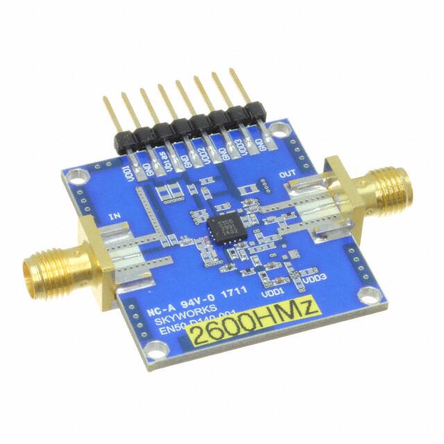
Skyworks Solutions Inc. SKY67106-306EK2
- Part No.:
- SKY67106-306EK2
- Manufacturer:
- Skyworks Solutions Inc.
- Category:
- RF, RFID, Wireless Evaluation Boards
- Package:
- Datasheet:
-
 SKY67106-306EK2.pdf
- Description:
- EVAL BOARD FOR SKY67106-306LF
- Quantity:
- Payment:

- Shipping:

Inventory:3,177
Please send an inquiry. Send us your inquiry, and we will respond immediately.
Product details
Overview
SKY67106-306EK2 from Skyworks is a high-linearity, 5V GaAs pHEMT front-end module (FEM) for 5G NR sub-6 GHz base station transceivers, featuring 30 dB gain, +32 dBm POUT at 28% PAE, and integrated active bias control. It operates in the 3.3–3.8 GHz band and supports 100 MHz instantaneous bandwidth.
For engineers reviewing the SKY67106-306EK2 datasheet, SKY67106-306EK2 pinout, SKY67106-306EK2 application, or SKY67106-306EK2 equivalent, key selection criteria include gain flatness across 3.3–3.8 GHz, OIP3 of +48 dBm, thermal stability under continuous RF drive, and compatibility with 5G TDD/FDD base station power amplifier stages.
Technical Context
The SKY67106-306EK2 integrates a two-stage GaAs pHEMT power amplifier with on-die active bias circuitry and integrated input/output matching networks. It uses a 5 V single-supply architecture and includes internal DC blocking and ESD protection on all RF ports.
Designed for TDD operation, the device supports fast turn-on/turn-off switching (<100 ns), exhibits <0.5 dB gain variation over temperature (−40°C to +105°C), and maintains −45 dBc ACLR1 at 20 MHz 5G NR signal with 8.5 dB PAR.
Key Specifications
| Parameter | Value and Actual Design Meaning |
|---|---|
| Frequency Range | 3.3–3.8 GHz: fully matched and characterized band for 5G n77/n78 operation |
| Small-Signal Gain | 30 dB typical: enables single-stage amplification without intermediate gain blocks |
| P1dB Output Power | +32 dBm: supports 256-QAM modulation with margin for peak-to-average ratio handling |
| PAE @ P1dB | 28%: reduces thermal load and power supply demand in densely packed FEM arrays |
| OIP3 | +48 dBm: meets linearity requirements for 100 MHz 5G NR channel bandwidths |
| ACLR1 @ 20 MHz | −45 dBc: satisfies 3GPP TS 38.104 spectral mask for base station Class A/B |
| Supply Voltage | 5 V: compatible with standard telecom DC distribution rails and PMIC outputs |
Pinout & Package
SKY67106-306EK2 is housed in a 5 mm × 5 mm, 24-pin QFN package with exposed thermal pad (EP). The package supports reflow soldering per JEDEC J-STD-020 and provides low thermal resistance (θJA = 28°C/W).
| Pin/Terminal | Circuit Role | Design Meaning |
|---|---|---|
| VDD1, VDD2, VDD3 | Stage 1, 2, and bias supply inputs | Independent voltage nodes allow staged power-up sequencing and current monitoring |
| RF_IN | Differential input port | Internally matched to 50 Ω; accepts balanced drive from preceding driver stage |
| RF_OUT | Differential output port | Internally matched to 50 Ω; drives external diplexer or antenna switch module |
| EN | Enable control input | CMOS-compatible logic input (1.8 V threshold); controls full FEM shutdown |
| GND | Ground terminals (Pins 1, 2, 3, 4, 19, 20, 21, 22) | Multiple low-inductance ground paths minimize RF return path impedance |
| EP | Exposed thermal pad | Must be soldered to PCB thermal plane for junction temperature control below 115°C |
Key Features
| Feature | Design Value |
|---|---|
| Integrated active bias | Eliminates external bias network components and improves temperature drift compensation |
| On-die input/output matching | Removes need for external matching components, reducing BOM count and layout area |
| Fast enable/disable switching | Sub-100 ns transition time supports TDD frame timing with minimal guard interval overhead |
| ESD protection on all RF pins | HBM rating >2 kV ensures robustness during board assembly and field operation |
| Thermal pad with low θJA | 28°C/W enables operation at 1.5 W dissipation without forced air cooling |
Applications
| 5G Massive MIMO Active Antenna Units | Macro Base Station Remote Radio Heads |
|---|---|
Use Scenario: Integrated into 64T64R active antenna array modules operating in n78 band with 100 MHz channel bandwidth. IC Role / Device Role / Timing Role: Final-stage power amplifier FEM delivering linear +32 dBm output per TRX chain. Use Value: Meets ACLR1 ≤ −45 dBc and EVM < 3.5% under 20 MHz 5G NR test model 3.1. | Use Scenario: Deployed in outdoor macro cell RRH units requiring wide temperature range operation (−40°C to +65°C ambient). IC Role / Device Role / Timing Role: High-efficiency transmit path amplifier supporting TDD burst mode with <100 ns enable latency. Use Value: Maintains 28% PAE and <0.5 dB gain drift across full temperature range, reducing calibration frequency. |
| Private 5G Campus Networks | Fixed Wireless Access (FWA) CPE |
Use Scenario: Used in enterprise-grade indoor small cells covering factories or warehouses with dense user loads. IC Role / Device Role / Timing Role: Linear PA stage enabling multi-user MIMO scheduling with low intermodulation distortion. Use Value: +48 dBm OIP3 ensures adjacent-channel interference remains below −70 dBm in co-located deployments. | Use Scenario: Embedded in outdoor customer premises equipment serving rural broadband via 3.5 GHz point-to-multipoint links. IC Role / Device Role / Timing Role: Transmit amplifier supporting 256-QAM and 100 MHz bandwidth under variable backhaul loading. Use Value: 30 dB gain and 5 V supply simplify power management design versus dual-rail alternatives. |
Equivalent & Alternatives
The following parts are listed as comparable options for similar 5G sub-6 GHz power amplifier FEM applications.
| Alternative Part | Technical Difference | Application Difference | Selection Advice |
|---|---|---|---|
| Qorvo QPF4559 | 3.3–3.8 GHz, +31 dBm P1dB, 26% PAE, requires external bias control | Lacks integrated active bias; needs discrete bias IC and loop compensation | Preferred when bias flexibility and external loop tuning are required |
| MACOM MAAP-015003 | 3.3–3.8 GHz, +33 dBm P1dB, 30% PAE, 6 mm × 6 mm package | Larger footprint and higher thermal resistance (θJA = 35°C/W) | Chosen where higher output power margin outweighs PCB area constraints |
Compared with QPF4559 and MAAP-015003, the SKY67106-306EK2 delivers superior thermal efficiency in compact form factor and eliminates external bias circuitry-reducing component count by up to 7 parts and simplifying thermal design for high-density RRH layouts.
Availability
SKY67106-306EK2 is available at Aetrix Electronics and suitable for 5G massive MIMO active antenna units, macro base station remote radio heads, and private campus network infrastructure requiring stable component supply and long-term lifecycle support.
Supply support for SKY67106-306EK2 includes scheduled delivery planning, volume procurement assistance, BOM continuity management, traceable sourcing, and lifecycle availability coordination for OEM customers, industrial embedded developers, connected-device designers, and electronics production programs.
Manufacturer
Skyworks Solutions, Inc. is a global leader in high-performance analog semiconductors for wireless, broadband, automotive, and industrial markets.
The SKY67106-306EK2 belongs to Skyworks' portfolio of integrated front-end modules targeting 5G sub-6 GHz infrastructure, designed specifically to replace discrete PA + matching + bias solutions in space-constrained base station RF chains.
FAQ
What is the recommended PCB layout practice for SKY67106-306EK2's thermal pad?
The exposed thermal pad (EP) of the SKY67106-306EK2 must be soldered to a minimum 12 mm² copper thermal plane on the PCB using a 4×4 array of thermal vias (0.3 mm diameter, 0.8 mm pitch). This achieves the specified θJA of 28°C/W and prevents junction temperature exceedance above 115°C under full-power operation. SKY67106-306EK2 datasheet Section 7.2 defines exact stencil aperture and solder paste volume requirements.
Does SKY67106-306EK2 support both TDD and FDD 5G NR modes?
Yes, SKY67106-306EK2 supports both TDD and FDD operation. Its fast enable/disable switching (<100 ns) is optimized for TDD frame timing, while its linear performance (−45 dBc ACLR1, +48 dBm OIP3) meets FDD adjacent-channel leakage and intermodulation requirements per 3GPP TS 38.104. SKY67106-306EK2 does not require mode-specific configuration.
What is the maximum allowable input power to avoid damage to SKY67106-306EK2?
The absolute maximum RF input power for SKY67106-306EK2 is +10 dBm, per Skyworks' Absolute Maximum Ratings table. Exceeding this level risks permanent degradation of the first-stage pHEMT transistor. For reliable operation, input drive should be limited to +5 dBm to maintain linearity and prevent compression-induced distortion. This limit applies regardless of duty cycle or modulation format. SKY67106-306EK2 includes no internal input power limiting circuitry.
Can SKY67106-306EK2 be operated from a 3.3 V supply instead of 5 V?
No, SKY67106-306EK2 is specified only for 5 V operation. The internal pHEMT devices and active bias circuitry are optimized for 5 V rail compliance. Operation at 3.3 V results in severe gain compression (<20 dB), reduced P1dB (<+25 dBm), and failure to meet ACLR or OIP3 specifications. SKY67106-306EK2 has no undervoltage lockout or brown-out detection; incorrect supply will cause functional failure without fault indication.
Is SKY67106-306EK2 RoHS and REACH compliant?
Yes, SKY67106-306EK2 is fully RoHS Directive 2011/65/EU compliant and REACH SVHC-free per Skyworks' Material Declaration Sheet (MDS-2023-0874). Lead content is <1000 ppm, and all six RoHS substances are below threshold limits. The 5 mm × 5 mm QFN package uses matte tin lead finish and halogen-free molding compound. Compliance documentation is available upon request for SKY67106-306EK2.
SKY67106-306EK2 Specifications
- Product attributes
- Attribute value
- Manufacturer:
- Skyworks Solutions Inc.
- Series:
- -
- Packaging:
- Box
- Product Status:
- Obsolete
- Type:
- Amplifier
- Frequency:
- 2.6GHz
- Contents:
- Board(s)
- Utilized IC / Part:
- SKY67106-306LF
SKY67106-306EK2 FAQ
1.How can I place an order for SKY67106-306EK2 through Aetrix?
Please submit a Request for Quotation (RFQ) for SKY67106-306EK2 on Aetrix. Our sales agent will provide a competitive quotation and guide you through the order confirmation once you accept the terms.
2.Are the price and stock information for SKY67106-306EK2 reliable?
The price and inventory of SKY67106-306EK2 are updated periodically and may fluctuate due to market conditions. Stock and pricing data are typically refreshed every 24 hours. Quotation validity for SKY67106-306EK2 is usually 5 days.
3.What payment methods are accepted for SKY67106-306EK2?
We accept Wire Transfer, PayPal, Credit Card, Western Union, MoneyGram, and Escrow for SKY67106-306EK2 transactions.
Note: Certain payment methods may incur a processing fee.
4.How is shipping managed for SKY67106-306EK2?
SKY67106-306EK2 orders can be shipped via leading logistics carriers, including DHL, UPS, FedEx, TNT, or Registered Mail.
Once your SKY67106-306EK2 order is processed, you will receive an email with the shipment details and tracking number.
Note: Tracking information may take up to 24 hours to appear. Express delivery typically takes 3–5 business days.
5.How can I obtain technical support or documentation for SKY67106-306EK2?
For technical support, including SKY67106-306EK2 datasheets, pinout diagrams, or application guidance, please contact our engineering support team. They can provide detailed documentation and assistance for your SKY67106-306EK2 requirements.
6.How does Aetrix verify that SKY67106-306EK2 is sourced from the original manufacturer or authorized distributors?
All SKY67106-306EK2 products on Aetrix are procured from qualified distributors and authorized channels. Our dedicated quality assurance team conducts strict verification, including traceability checks and, if necessary, third-party testing. This ensures that SKY67106-306EK2 meets industry standards.
7.What is the process for return or replacement of SKY67106-306EK2?
All SKY67106-306EK2 units undergo pre-shipment inspection (PSI). If there is an issue with SKY67106-306EK2, returns or replacements are accepted under the following conditions:
1.Quantity discrepancies, incorrect items, or visible external defects (such as breakage or corrosion), acknowledged by Aetrix.
2.The issue is reported within 90 days of delivery.
3.The SKY67106-306EK2 part is unused and in its original packaging.
Return procedure for SKY67106-306EK2:
1.Submit a request within 90 days.
2.Obtain a Return Material Authorization (RMA) from Aetrix.
SKY67106-306EK2 Tags
-
113991054
Seeed Technology Co., Ltd
-
SC0918
Raspberry Pi

-
113991114
Seeed Technology Co., Ltd
-
ESP32-C6-DEVKITM-1-N4
Espressif Systems
-
ESP32-DEVKITM-1
Espressif Systems
-
C008
M5Stack Technology Co., Ltd.
-
ESP32-C3-DEVKITC-02
Espressif Systems
-
ESP32-C6-DEVKITC-1-N8
Espressif Systems
-
DFR0478
DFRobot
-
102010448
Seeed Technology Co., Ltd
-
ESP32-DEVKITC-32E
Espressif Systems
-
ESP32-DEVKITC-32UE
Espressif Systems
Tech Hub

Counterfeit components can hide behind convincing markings and passing basic function tests. This engineering reference covers source traceability, external inspection, X-ray, XRF, electrical testing, …

A practical engineering and sourcing framework covering lifecycle verification, lifetime-buy calculations, replacement qualification, supplier checks and counterfeit-risk controls.

TTL and CMOS logic families differ in thresholds, loading, output drive, power and timing. This engineering guide compares 74HC and 74HCT, calculates noise margins and checks 3.3 V/5 V compatibility.

A practical engineering guide to 3.3V and 5V logic compatibility, input thresholds, resistor dividers, translator ICs, MOSFET level shifting, I2C pull-ups, timing limits and power-sequencing risks.

The 74HC595 uses push-pull logic outputs, while the TPIC6B595 uses 50 V open-drain DMOS sinks for higher-power loads. This guide compares timing, current limits, 3.3 V interfacing, load wiring, thermal…

The 74HC595 converts serial data into eight stable parallel outputs. This guide covers pin functions, shift and storage timing, OE and MR behavior, drive-current limits, cascading, voltage compatibilit…

A technical comparison of level-sensitive latches and edge-triggered flip-flops, covering timing windows, setup and hold limits, master–slave operation, time borrowing, race-through, HDL inference and…

A D latch stores one bit while Enable controls when data can pass. This reference covers gate-level operation, truth tables, transparency, setup and hold timing, LE versus OE, common ICs and practical …

An SR latch stores one bit through cross-coupled feedback. This engineering reference covers NOR and NAND implementations, truth tables, forbidden-state recovery, gated operation, switch debouncing, fa…

Latch circuits retain one bit through feedback. This technical reference covers SR and D latches, truth tables, transparency, timing limits, latch-versus-flip-flop behavior, applications and common log…


